Rev. 1.71 102 April 11, 2017 Rev. 1.71 103 April 11, 2017
HT66F002/HT66F0025/HT66F003/HT66F004
Cost-Effective A/D Flash MCU with EEPROM
HT66F002/HT66F0025/HT66F003/HT66F004
Cost-Effective A/D Flash MCU with EEPROM
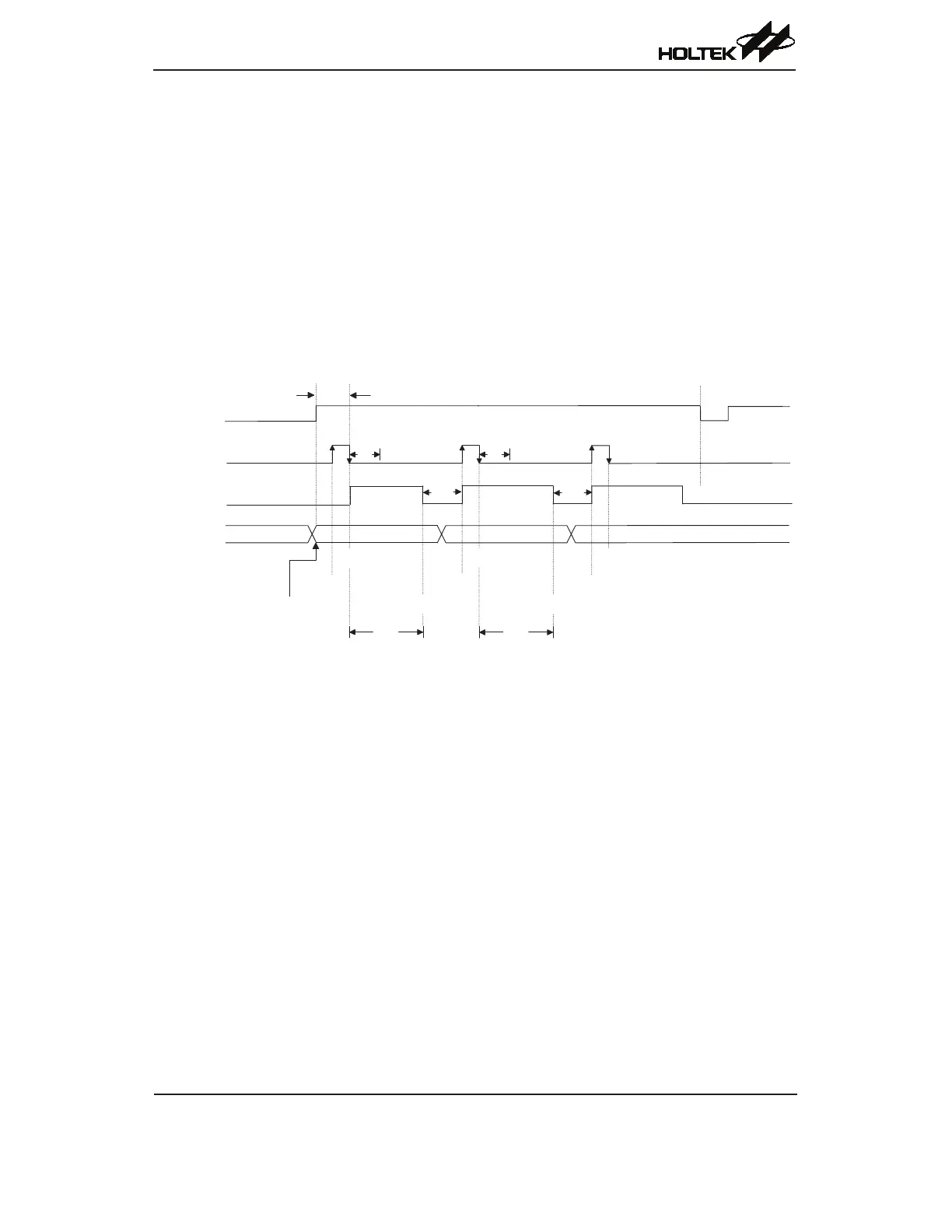
Conversion Rate and Timing Diagram
AcompleteA/Dconversioncontainstwoparts,datasamplinganddataconversion.Thedata
samplingwhichisdenedast
ADS
takes4A/Dclockcyclesandthedataconversiontakes12A/D
clockcycles.Thereforeatotalof16A/DclockcyclesforanA/Dconversionwhichisdenedast
ADC
arenecessary.
MaximumsingleA/Dconversionrate=A/Dclockperiod/16
However,thereisausagelimitationonthenextA/Dconversionafterthecurrentconversionis
complete.WhenthecurrentA/Dconversioniscomplete,theconverteddigitaldatawillbestored
intheA/DdataregisterpairandthenlatchedafterhalfanA/Dclockcycle.IftheSTARTbitisset
to1inhalfanA/DclockcycleaftertheendofA/Dconversion,theconverteddigitaldatastored
intheA/Ddataregisterpairwillbechanged.Therefore,itisrecommendedtoinitiatethenextA/D
conversionafteracertainperiodgreaterthanhalfanA/Dclockcycle attheendofcurrentA/D
conversion.
A/D Conversion Timing