Rev. 1.71 14 April 11, 2017 Rev. 1.71 15 April 11, 2017
HT66F002/HT66F0025/HT66F003/HT66F004
Cost-Effective A/D Flash MCU with EEPROM
HT66F002/HT66F0025/HT66F003/HT66F004
Cost-Effective A/D Flash MCU with EEPROM
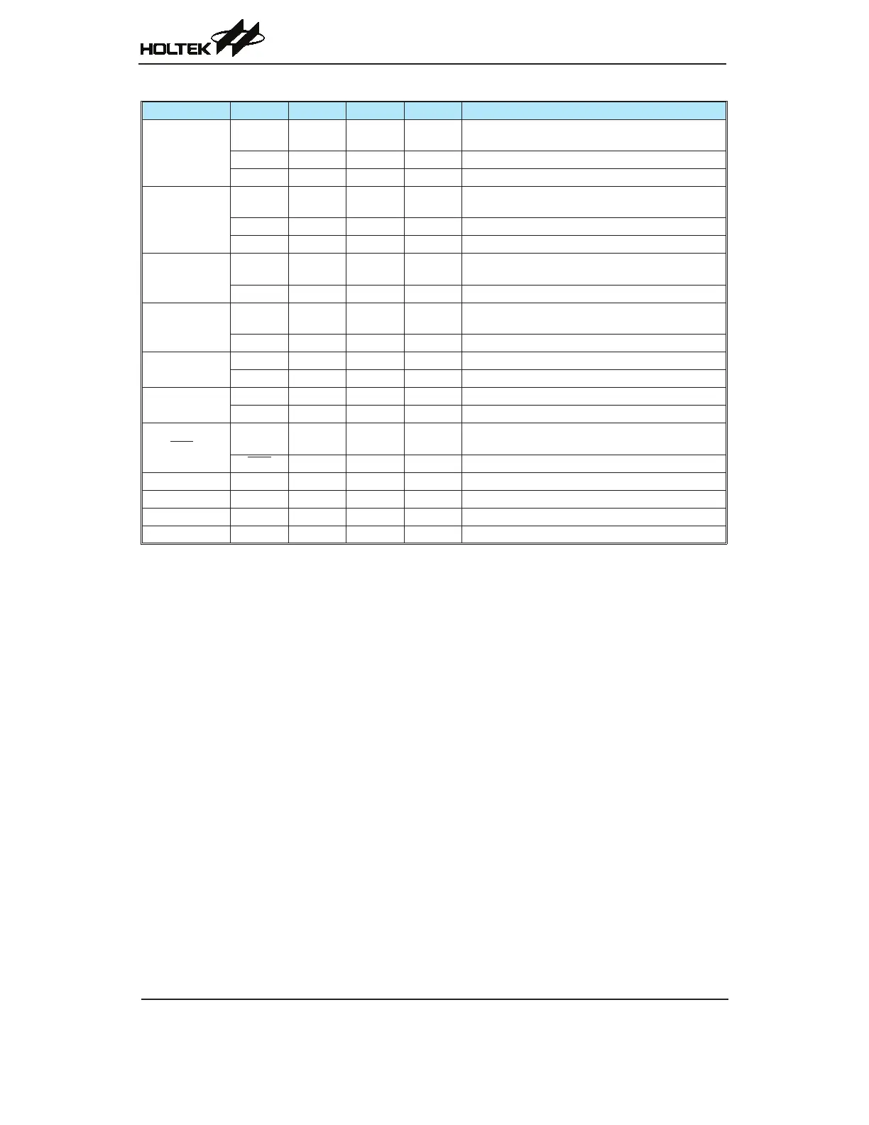
Pin Name Function OPT I/T O/T Description
PB3/SCOM3/
AN7
PB3
PBPU
PBSR
ST CMOS General purpose I/O. Register enabled pull-up
SCOM3 SCOMC — SCOM LCD driver output for LCD panel common
AN7 PBSR AN — ADC input channel 7
PB4/CLO/
SCOM2
PB4
PBPU
PBSR
ST CMOS General purpose I/O. Register enabled pull-up
CLO PBSR — CMOS System clock output
SCOM2 SCOMC — SCOM LCD driver output for LCD panel common
PB5/PTP0B
PB5
PBPU
PBSR
ST CMOS General purpose I/O. Register enabled pull-up
PTP0B PBSR ST CMOS PTM0 inverting output
PB6/PTP1B
PB6
PBPU
PBSR
ST CMOS General purpose I/O. Register enabled pull-up
PTP1B PBSR ST CMOS PTM1 inverting output
PC0/SCOM0
PC0 PCPU ST CMOS General purpose I/O. Register enabled pull-up
SCOM0 SCOMC — SCOM LCD driver output for LCD panel common
PC1/SCOM1
PC1 PCPU ST CMOS General purpose I/O. Register enabled pull-up
SCOM1 SCOMC — SCOM LCD driver output for LCD panel common
PC2/RES
PC1
PCPU
RSTC
ST CMOS General purpose I/O. Register enabled pull-up
RES RSTC ST — External reset input
VDD VDD — PWR — Digital positive power supply
AVDD AVDD — PWR — Analog positive power supply
VSS VSS — PWR — Digital negative power supply
AVSS AVSS — PWR — Analog negative power supply
Legend:I/T:Inputtype; O/T:Outputtype; PWR:Power;
OP:Optionalbyregisteroption SCOM:SoftwarecontrolledLCDCOM
ST:SchmittTriggerinput; CMOS:CMOSoutput; AN:Analogpin
*:VDDisthedevicepowersupplywhileAVDDistheADCpowersupply.TheAVDDpinisbonded
togetherinternallywithVDD.
**:VSSisthedevicegroundpinwhileAVSSistheADCgroundpin.TheAVSSpinisbondedtogether
internallywithVSS.
Absolute Maximum Ratings
SupplyVoltage................................................................................................V
SS
−0.3VtoV
SS
+6.0V
InputVoltage..................................................................................................V
SS
−0.3VtoV
DD
+0.3V
StorageTemperature....................................................................................................-50˚Cto125˚C
OperatingTemperature..................................................................................................-40˚Cto85˚C
I
OL
Total..................................................................................................................................... 80mA
I
OH
Total....................................................................................................................................-80mA
TotalPowerDissipation......................................................................................................... 500mW
Note:Thesearestressratingsonly.Stressesexceedingtherangespecifiedunder"AbsoluteMaximum
Ratings"maycausesubstantialdamagetothesedevices.Functionaloperationofthesedevicesat
otherconditionsbeyondthoselistedinthespecicationisnotimpliedandprolongedexposureto
extremeconditionsmayaffectdevicesreliability.