Rev. 1.71 66 April 11, 2017 Rev. 1.71 67 April 11, 2017
HT66F002/HT66F0025/HT66F003/HT66F004
Cost-Effective A/D Flash MCU with EEPROM
HT66F002/HT66F0025/HT66F003/HT66F004
Cost-Effective A/D Flash MCU with EEPROM
TM Interrupts
TheStandardandPeriodictypeTMseachhastwointernalinterrupts,theinternalcomparatorAor
comparatorP,whichgenerateaTMinterruptwhenacomparematchconditionoccurs.WhenaTM
interruptisgenerated,itcanbeusedtoclearthecounterandalsotochangethestateoftheTMoutputpin.
TM External Pins
EachoftheTMs,irrespectiveofwhattype,hastwoTMinputpins,withthelabelxTCKnand
xTPnI.TheTMinputpinxTCKn,isessentiallyaclocksourcefortheTMandisselectedusingthe
xTnCK2~xTnCK0bitsinthexTMnC0register.ThisexternalTMinputpinallowsanexternalclock
sourcetodrivetheinternalTM.ThisexternalTMinputpinissharedwithotherfunctionsbutwill
beconnectedtotheinternalTMifselectedusingthexTnCK2~xTnCK0bits.TheTMinputpincan
bechosentohaveeitherarisingorfallingactiveedge.
TheotherTMinputpin,xTPnI,isthecaptureinputwhoseactiveedgecanbearisingedge,afalling
edgeorbothrisingandfallingedgesandtheactiveedgetransitiontypeisselectedusingthexTnIO1
andxTnIO0bitsinthexTMnC1register.
TheTMseachhave twooutputpins withthelabelxTPnandxTPnB.WhentheTMisinthe
CompareMatchOutputMode,thesepinscanbecontrolledbytheTMtoswitchtoahighorlow
levelortotogglewhenacomparematchsituationoccurs.TheexternalxTPnoutputpinisalsothe
pinwheretheTMgeneratesthePWMoutputwaveform.AstheTMoutputpinsarepin-sharedwith
otherfunction,theTMoutputfunctionmustrstbesetupusingregisters.Asinglebitinoneofthe
registersdeterminesifitsassociatedpinistobeusedasanexternalTMoutputpinorifitistohave
anotherfunction.ThenumberofoutputpinsforeachTMtypeisdifferent,thedetailsareprovided
intheaccompanyingtable.
Device TM0 TM1
HT66F002/HT66F0025
STCK0, STP0I
STP0, STP0B
—
HT66F003
STCK0, STP0I
STP0, STP0B
PTCK1, PTP1I
PTP1, PTP1B
HT66F004
PTCK0, PTP0I
PTP0, PTP0B
PTCK1, PTP1I
PTP1, PTP1B
TM Input/Output Pins
TM Input/Output Pin Control Register
SelectingtohaveaTMinput/outputorwhethertoretainitsothersharedfunctionisimplemented
usingoneregister,withasinglebitineachregistercorrespondingtoaTMinput/outputpin.
ConguringtheselectionbitscorrectlywillsetupthecorrespondingpinasaTMinput/output.The
detailsofthepin-sharedfunctionselectionaredescribedinthepin-sharedfunctionsection.
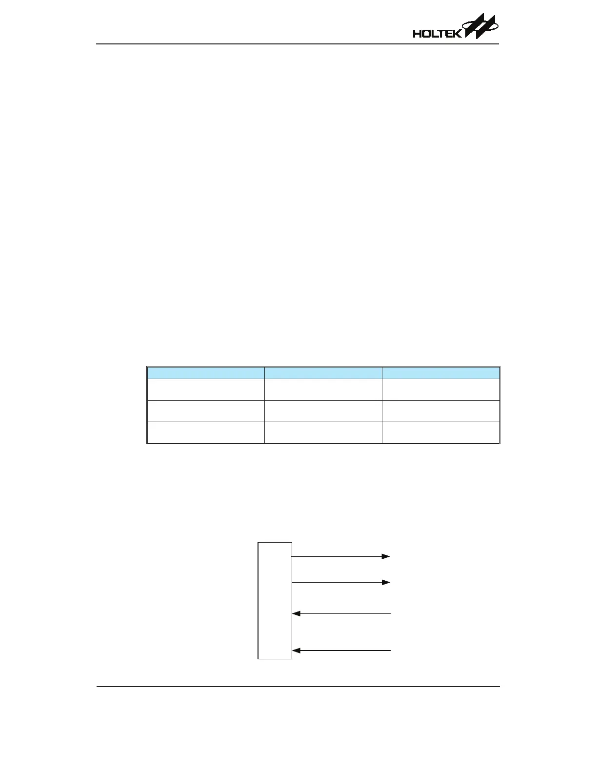
STM
STP0
STCK0
Capture Input
TCK Input
Output
STP0I
STP0B
Inverting Output
STM Function Pin Control Block Diagram