Rev. 1.71 96 April 11, 2017 Rev. 1.71 97 April 11, 2017
HT66F002/HT66F0025/HT66F003/HT66F004
Cost-Effective A/D Flash MCU with EEPROM
HT66F002/HT66F0025/HT66F003/HT66F004
Cost-Effective A/D Flash MCU with EEPROM
Analog to Digital Converter
Theneedtointerfacetorealworldanalogsignalsisacommonrequirementformanyelectronic
systems.However,toproperlyprocessthesesignalsbyamicrocontroller,theymustfirstbe
convertedintodigitalsignalsbyA/Dconverters.ByintegratingtheA/Dconversionelectronic
circuitryintothemicrocontroller,theneedforexternalcomponentsisreducedsignicantlywiththe
correspondingfollow-onbenetsoflowercostsandreducedcomponentspacerequirements.
A/D Overview
Thedevicescontainamulti-channelanalogtodigitalconverterwhichcandirectlyinterface
toexternalanalogsignals,suchasthatfromsensorsorothercontrolsignalsandconvertthese
signalsdirectlyintoa12-bitdigitalvalue.Theexternalorinternalanalogsignaltobeconvertedis
determinedbytheSAINSandSACSbitelds.Notethatwhentheinternalanalogsignalistobe
converted,thepin-sharedcontrolbitsshouldalsobeproperlyconfiguredexcepttheSAINSand
SACSbitfields.MoredetailedinformationabouttheA/Dinputsignalisdescribedinthe“A/D
ConverterControlRegisters”and“A/DConverterInputSignal”sectionsrespectively.
Part No. Input Channels A/D Channel Select Bits Input Pins
HT66F002
HT66F0025
HT66F003
4
SAINS2~SAINS0,
SACS1~SACS0
AN0~AN3
HT66F004 8
SAINS2~SAINS0,
SACS2~SACS0
AN0~AN7
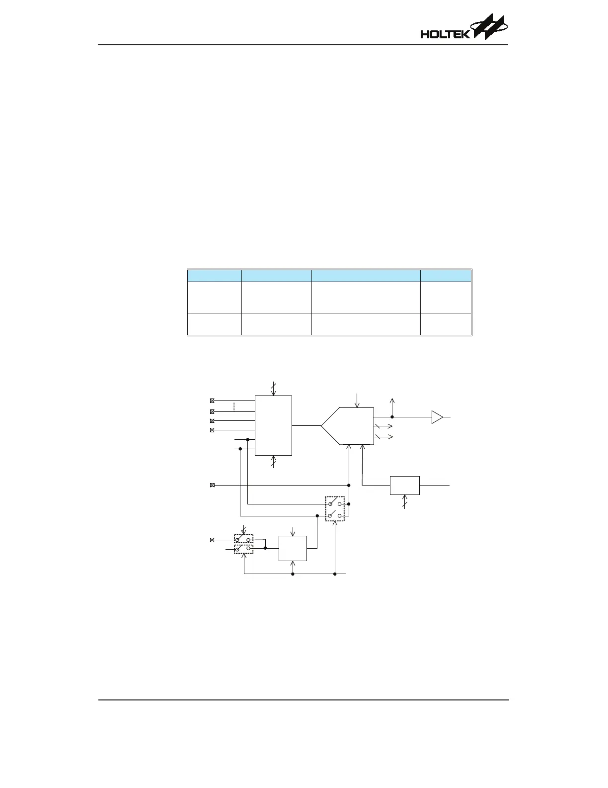
TheaccompanyingblockdiagramshowstheoverallinternalstructureoftheA/Dconverter,together
withitsassociatedregisters.
AN0
AN5
AN6
AN7
12-bit
SAR ADC
ENADC
SADOH[7:0]
SADOL[7:0]
ADBZ
SAINT
SACS[2:0]
V
BG
(1.04V)
VREF
V
RI
Divider
f
SYS
SACKS[2:0]
AV
DD
SAVRS[3:0]
V
R
VREFO
SAINS[2:0]
SAPIN
VREFO
ENOPA
PASR
OPA
MUX
Pin-shared selection
AV
DD
V
R
A/D Converter Structure