Rev. 1.71 76 April 11, 2017 Rev. 1.71 77 April 11, 2017
HT66F002/HT66F0025/HT66F003/HT66F004
Cost-Effective A/D Flash MCU with EEPROM
HT66F002/HT66F0025/HT66F003/HT66F004
Cost-Effective A/D Flash MCU with EEPROM
Timer/Counter Mode
Toselectthismode,bitsST0M1andST0M0intheSTM0C1registershouldbesetto11
respectively.TheTimer/CounterModeoperatesinanidenticalwaytotheCompareMatchOutput
Modegeneratingthesameinterruptflags.TheexceptionisthatintheTimer/CounterModethe
STMoutputpinisnotused.ThereforetheabovedescriptionandTimingDiagramsfortheCompare
MatchOutputModecanbeusedtounderstanditsfunction.AstheSTMoutputpinisnotusedin
thismode,thepincanbeusedasanormalI/Opinorotherpin-sharedfunctionbysettingpin-share
functionregister.
PWM Output Mode
Toselectthismode,bitsST0M1andST0M0intheSTM0C1registershouldbesetto10respectively
andalsotheST0IO1andST0IO0bitsshouldbesetto10respectively.ThePWMfunctionwithin
theSTMisusefulforapplicationswhichrequirefunctionssuchasmotorcontrol,heatingcontrol,
illuminationcontroletc.Byprovidingasignalofxedfrequencybutofvaryingdutycycleonthe
STMoutputpin,asquarewaveACwaveformcanbegeneratedwithvaryingequivalentDCRMS
values.
AsboththeperiodanddutycycleofthePWMwaveformcanbecontrolled,thechoiceofgenerated
waveformisextremelyexible.InthePWMoutputmode,theST0CCLRbithasnoeffectasthe
PWMperiod.BothoftheCCRAandCCRPregistersareusedtogeneratethePWMwaveform,one
registerisusedtocleartheinternalcounterandthuscontrolthePWMwaveformfrequency,while
theotheroneisusedtocontrolthedutycycle.Whichregisterisusedtocontroleitherfrequency
ordutycycleisdeterminedusingtheST0DPXbitintheSTM0C1register.ThePWMwaveform
frequencyanddutycyclecanthereforebecontrolledbythevaluesintheCCRAandCCRPregisters.
Aninterruptag,oneforeachoftheCCRAandCCRP,willbegeneratedwhenacomparematch
occursfromeitherComparatorAorComparatorP.TheST0OCbitintheSTM0C1registerisused
toselecttherequiredpolarityofthePWMwaveformwhilethetwoST0IO1andST0IO0bitsare
usedtoenablethePWMoutputortoforcetheSTMoutputpintoaxedhighorlowlevel.The
ST0POLbitisusedtoreversethepolarityofthePWMoutputwaveform.
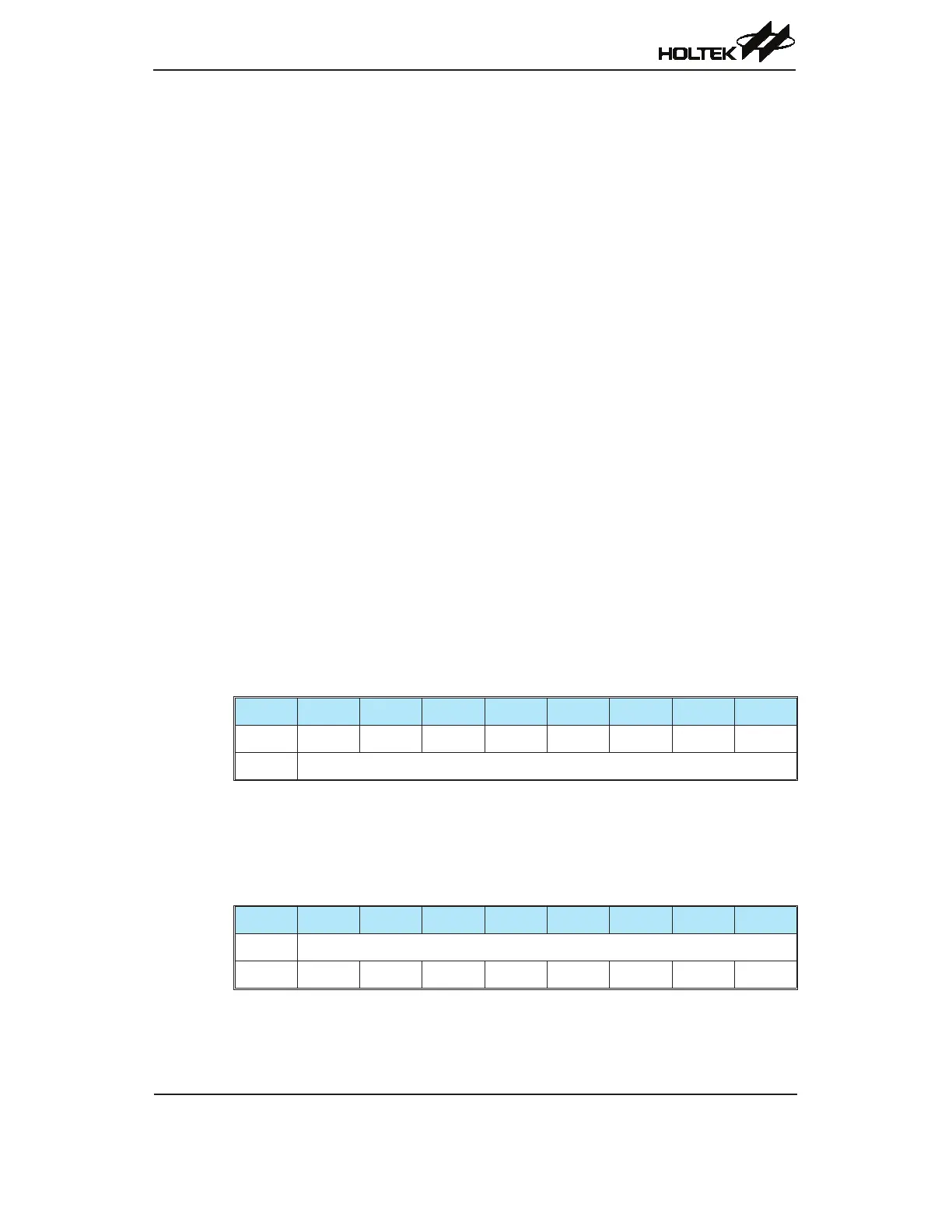
• 10-bit STM, PWM Output Mode, Edge-aligned Mode, ST0DPX=0
CCRP 001b 010b 011b 100b 101b 110b 111b 000b
Period 128 256 384 512 640 768 896 1024
Duty CCRA
Iff
SYS
=16MHz,TMclocksourceisf
SYS
/4,CCRP=100bandCCRA=128,
TheSTMPWMoutputfrequency=(f
SYS
/4)/512=f
SYS
/2048=7.8125kHz,duty=128/512=25%.
IftheDutyvaluedenedbytheCCRAregisterisequaltoorgreaterthanthePeriodvalue,thenthe
PWMoutputdutyis100%.
• 10-bit STM, PWM Output Mode, Edge-aligned Mode, ST0DPX=1
CCRP 001b 010b 011b 100b 101b 110b 111b 000b
Period CCRA
Duty 128 256 384 512 640 768 896 1024
ThePWMoutputperiodisdeterminedbytheCCRAregistervaluetogetherwiththeSTMclock
whilethePWMdutycycleisdenedbytheCCRPregistervalue.