Rev. 1.71 24 April 11, 2017 Rev. 1.71 25 April 11, 2017
HT66F002/HT66F0025/HT66F003/HT66F004
Cost-Effective A/D Flash MCU with EEPROM
HT66F002/HT66F0025/HT66F003/HT66F004
Cost-Effective A/D Flash MCU with EEPROM
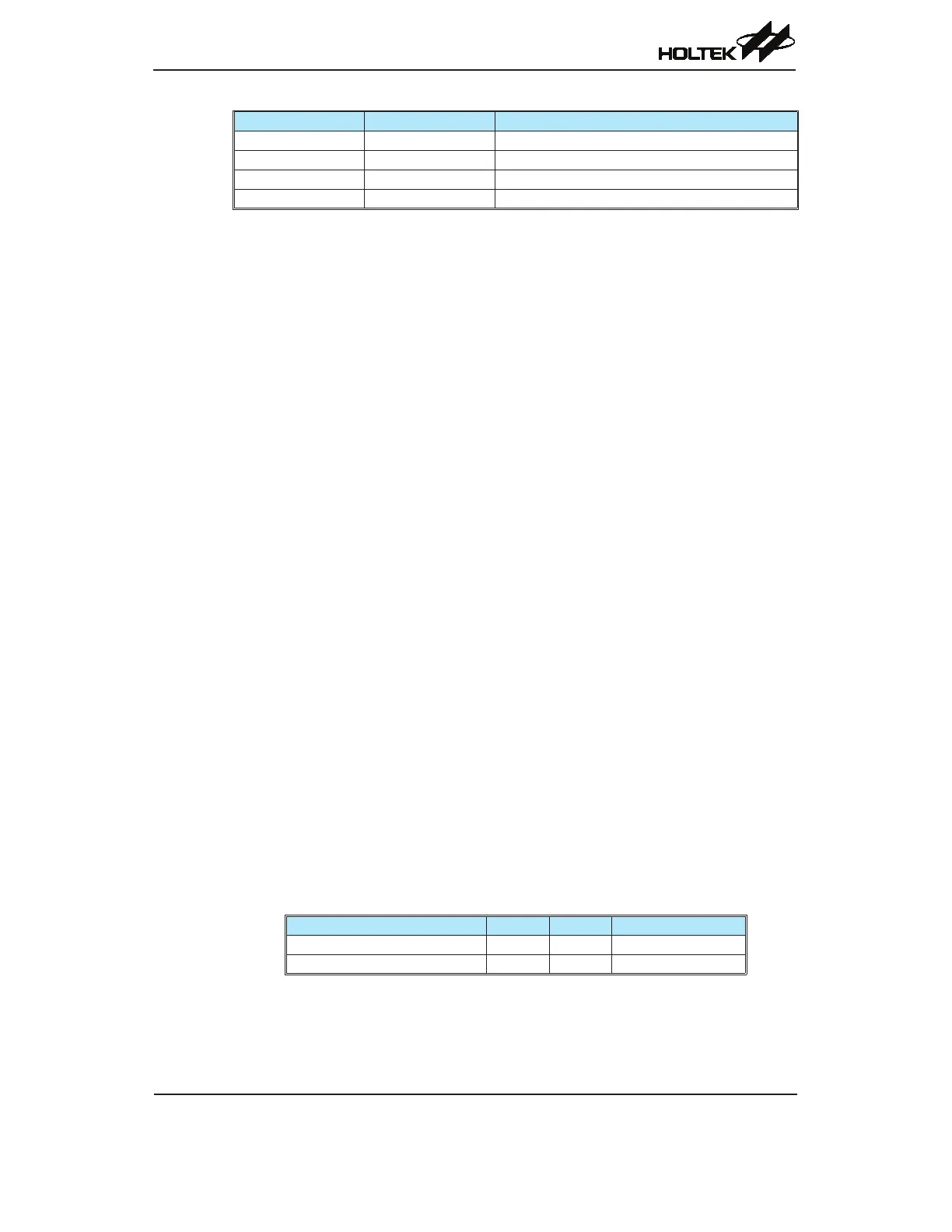
Holtek e-Link Pins EV Chip Pins Pin Description
OCDSDA OCDSDA On-chip Debug Support Data/Address input/output
OCDSCK OCDSCK On-chip Debug Support Clock input
VDD VDD Power Supply
GND VSS Ground
RAM Data Memory
TheDataMemoryisavolatileareaof8-bitwideRAMinternalmemoryandisthelocationwhere
temporaryinformationisstored.
Structure
Dividedintotwosections,therstoftheseisanareaofRAM,knownastheSpecialFunctionData
Memory.Herearelocatedregisterswhicharenecessaryforcorrectoperationofthedevice.Many
oftheseregisterscanbereadfromandwrittentodirectlyunderprogramcontrol,however,some
remainprotectedfromusermanipulation.ThesecondareaofDataMemoryisknownastheGeneral
PurposeDataMemory,whichisreservedforgeneralpurposeuse.Alllocationswithinthisareaare
readandwriteaccessibleunderprogramcontrol.
TheoverallDataMemoryissubdividedintotwobanks.TheSpecialPurposeDataMemoryregisters
areaccessibleinallbanks,withtheexceptionoftheEECregisterataddress40H,whichisonly
accessibleinBank1.SwitchingbetweenthedifferentDataMemorybanksisachievedbysettingthe
BankPointertothecorrectvalue.ThestartaddressoftheDataMemoryforalldevicesistheaddress
00H.
General Purpose Data Memory
Thereis64or96bytesofgeneralpurposedatamemorywhicharearrangedinBank0andBank1.
Allmicrocontrollerprogramsrequireanareaofread/writememorywheretemporarydatacanbe
storedandretrievedforuselater.ItisthisareaofRAMmemorythatisknownasGeneralPurpose
DataMemory.ThisareaofDataMemoryisfullyaccessiblebytheuserprogramingforbothreading
andwritingoperations.Byusingthebitoperationinstructionsindividualbitscanbesetorreset
underprogramcontrolgivingtheuseralargerangeofexibilityforbitmanipulationintheData
Memory.
Special Purpose Data Memory
ThisareaofDataMemoryiswhereregisters,necessaryforthecorrectoperationofthe
microcontroller,arestored.Mostoftheregistersarebothreadableandwriteablebutsomeare
protectedandarereadableonly,thedetailsofwhicharelocatedundertherelevantSpecialFunction
Registersection.Notethatforlocationsthatareunused,anyreadinstructiontotheseaddresseswill
returnthevalue“00H”.
Device Capacity Bank 0 Bank 1
HT66F002/HT66F0025/HT66F003 64×8 40H~7FH 40H EEC register only
HT66F004 96×8 40H~9FH 40H EEC register only