Rev. 1.71 24 April 11, 2017 Rev. 1.71 25 April 11, 2017
HT66F002/HT66F0025/HT66F003/HT66F004
Cost-Effective A/D Flash MCU with EEPROM
HT66F002/HT66F0025/HT66F003/HT66F004
Cost-Effective A/D Flash MCU with EEPROM
In Circuit Programming – ICP
TheprovisionofFlashtypeProgramMemoryprovidestheuserwithameansofconvenientandeasy
upgradesandmodicationstotheirprogramsonthesamedevice.Asanadditionalconvenience,
Holtekhasprovidedameansofprogrammingthemicrocontrollerin-circuitusinga4-pininterface.
Thisprovidesmanufacturerswiththepossibilityofmanufacturingtheircircuitboardscompletewith
aprogrammedorun-programmedmicrocontroller,andthenprogrammingorupgradingtheprogram
atalaterstage.Thisenablesproductmanufacturerstoeasilykeeptheirmanufacturedproducts
suppliedwiththelatestprogramreleaseswithoutremovalandre-insertionofthedevice.
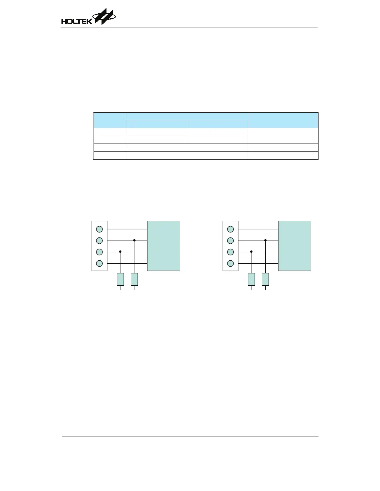
Holtek
Write Pins
MCU Programming Pins
Function
HT66F002/HT66F0025 HT66F003/HT66F004
ICPDA PA0 Programming Serial Data
ICPCK PA7 PA2 Programming Serial Clock
VDD VDD Power Supply
VSS VSS Ground
TheProgramMemoryandEEPROMdatamemorycanbothbeprogrammedseriallyin-circuitusing
this4-wireinterface.Dataisdownloadedanduploadedseriallyonasinglepinwithanadditional
linefortheclock.Twoadditionallinesarerequiredforthepowersupplyandground.Thetechnical
detailsregardingthein-circuitprogrammingofthedevicearebeyondthescopeofthisdocument
andwillbesuppliedinsupplementaryliterature.
HT66F002/HT66F0025
* *
Writer_VDD
ICPDA
ICPCK
Writer_VSS
To other Circuit
VDD
PA0
PA7
VSS
Writer Connector
Signals
MCU Programming
Pins
HT66F003/HT66F004
* *
Writer_VDD
ICPDA
ICPCK
Writer_VSS
To other Circuit
VDD
PA0
PA2
VSS
Writer Connector
Signals
MCU Programming
Pins
Note:*mayberesistororcapacitor.Theresistanceof*mustbegreaterthan1korthecapacitanceof*mustbe
lessthan1nF.
On-Chip Debug Support – OCDS
ThereisanEVchipwhichisusedtoemulatetheHT66F00xdeviceseries.ThisEVchipdevice
alsoprovidesan“On-ChipDebug”functiontodebugthedeviceduringthedevelopmentprocess.
TheEVchipandtheactualMCUdevicesarealmostfunctionallycompatibleexceptforthe“On-
ChipDebug”function.UserscanusetheEVchipdevicetoemulatetherealchipdevicebehavior
byconnectingtheOCDSDAandOCDSCKpinstotheHoltekHT-IDEdevelopmenttools.The
OCDSDApinistheOCDSData/Addressinput/outputpinwhiletheOCDSCKpinistheOCDS
clockinputpin.WhenusersusetheEVchipfordebugging,otherfunctionswhicharesharedwith
theOCDSDAandOCDSCKpinsintheactualMCUdevicewillhavenoeffectintheEVchip.
However,thetwoOCDSpinswhicharepin-sharedwiththeICPprogrammingpinsarestillusedas
theFlashMemoryprogrammingpinsforICP.ForamoredetailedOCDSdescription,refertothe
correspondingdocumentnamed“Holteke-Linkfor8-bitMCUOCDSUser’sGuide”.