Service
Model
83522A
Check TP3 for the Birdie signal illustrated in Figure 8-57. (The birdie can be
centered on the screen with the front panel
FREQ
CAL
knob.) If the waveform
is incorrect, refer to A8 troubleshooting.
Check TP2 for the waveform shown in Figure 8-57. These Marker OFF pulses
should surround the Marker ON pulses at
TP1. If these are incorrect, check the
outputs of the monostable multivibrators against the data in Table 8-12.
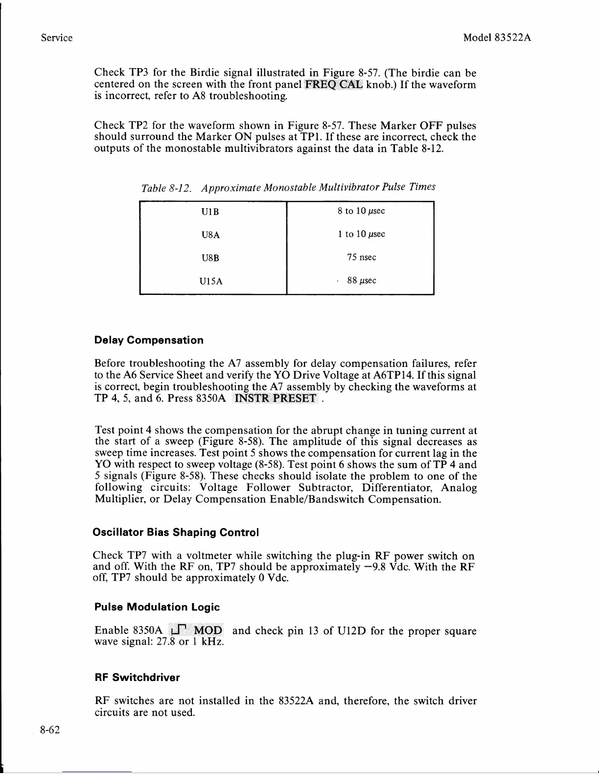
Table
8-12.
Approximate Monostable Multivibrator Pulse Times
Delay Compensation
U1B
U8A
U8B
U15A
i
Before troubleshooting the A7 assembly for delay compensation failures, refer
to the A6 Service Sheet and verify the YO Drive Voltage at
A6TP14. If this signal
is correct, begin troubleshooting the A7 assembly by checking the waveforms at
TP 4, 5, and 6. Press
8350A
INSTR
PRESET
.
8
to
10
psec
1
to
10
psec
75
nsec
rn
88
psec
Test point 4 shows the compensation for the abrupt change in tuning current at
the start of a sweep (Figure 8-58). The amplitude of this signal decreases as
sweep time increases. Test point 5 shows the compensation for current lag in the
YO with respect to sweep voltage (8-58). Test point 6 shows the sum of TP 4 and
5 signals (Figure 8-58). These checks should isolate the problem to one of the
following circuits: Voltage Follower Subtractor, Differentiator, Analog
Multiplier, or Delay Compensation
EnableIBandswitch Compensation.
Oscillator Bias Shaping Control
Check TP7 with a voltmeter while switching the plug-in RF power switch on
and off. With the
RF
on, TP7 should be approximately
-9.8
Vdc. With the RF
off, TP7 should be approximately
0
Vdc.
Pulse Modulation Logic
Enable 8350A
and check pin 13 of U12D for the proper square
wave signal: 2
RF
Switchdriver
RF switches are not installed in the 83522A and, therefore, the switch driver
circuits are not used.
 Loading...


