Chapter 6 Function Introduction Shenzhen Hpmont Technology Co., Ltd
―90― HD30 Series Inverters User Manual
No. Name Description Range
factory setting
F15.24 Output terminal positive and negative logic selection 00
0x3F
0
It defines that each bit (binary) of this function represents different physical sources.
• Positive logic: When multi-function output terminals are connected to corresponding common
port, this logic is enabled. Otherwise the logic is disabled.
• Negative logic: When multi-function output terminals are connected to corresponding common
port, this logic is disabled. Otherwise the logic is enabled.
Tens Units
Bit7 Bit6 Bit5 Bit4 Bit3 Bit2 Bit1 Bit0
- - RLY4 RLY3 RLY2 RLY1 DO2 DO1
• 0 means positive logic while 1 means negative logic.
Note: Only when using HD30-EIO will RLY2
RLY4 be enabled.
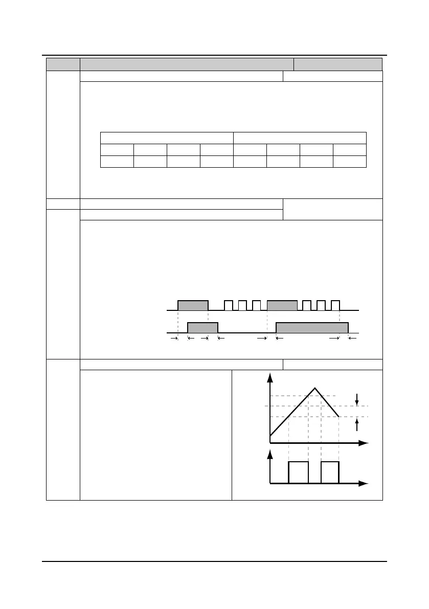
F15.25 ON side delay time of timing function 0.00
300.00s
0.00
OFF side delay time of timing function
F15.25 and F15.26 can be used to set the ON/OFF side delay time (dead area) of the timing function
output relative to the input.
• The timing function output will be ON when the ON time of timing function is longer than that
defined by F15.25.
• The timing function output will be OFF when the OFF time of timing function delays behind that
defined by F15.26.
The timing function operation figure is shown as follows:
F15.27 FAR range 0.10
100.00Hz
2.50
The pulse signal will be output if the inverter’s
output frequency is within the FAR range. As
shown in the right figure.
ON ON
ON ON
Timing function input
Timing function output
F15.25 F15.25F15.26 F15.26
Output
Detecting range
Preset
frequency
Time
Time
DO
 Loading...