User’s Manual
IBM PowerPC 750GX and 750GL RISC Microprocessor
gx_08.fm.(1.2)
March 27, 2006
Bus Interface Operation
Page 313 of 377
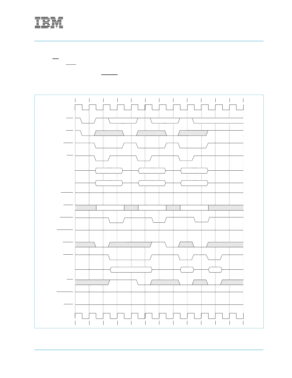
Figure 8-20 shows data-delay controls in a single-beat write operation. Note that all bidirectional signals are
tristated between bus tenures. Data transfers are delayed in the following ways:
• The TA
signal is held negated to insert wait states in clocks 3 and 4.
• In clock 6, DBG
is held negated, delaying the start of the data tenure.
The last access is not delayed (DRTRY
is valid only for read operations).
Figure 8-20. Single-Beat Writes Showing Data-Delay Controls
BR
BG
ABB
TS
A[0–31]
TT[0–4]
TBST
GBL
AACK
ARTRY
DBG
DBB
D[0–63]
TA
DRTRY
TEA
1 2 3 4 5 6 7 8 9 10 11 12
1 2 3 4 5 6 7 8 9 10 11 12
CPU A CPU A CPU A
SBW SBW SBW
Out Out Out

 Loading...


