P/N 960-000180R_Rev. 1 {EDP #233427} © 2016, JAPAN CASH MACHINE CO., LTD.
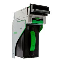
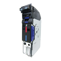
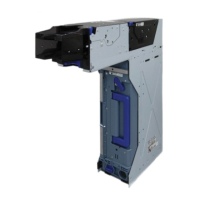
Installation DBV® Series DBV-400 Banknote Validator Section 2
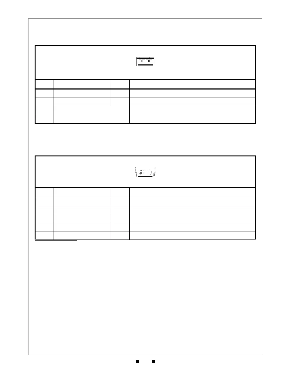
USB Interface Connector Pin Assignments
Table 2-10 lists the DBV-400 USB Interface Connector Pin Assignments.
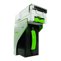
USB Maintenance Interface Connector Pin Assignment
Table 2-11 lists the DBV-400 USB Maintenance Interface Connector Pin Assignments.
Table 2-10 DBV-400 USB Interface Connector Pin Assignments
CN2 Connector (DBV-400 Side):S4B-XH-A (JST)
Housing (Cable Side): XHP-4B (JST)
Contact (Cable Side): SXH-001T-PO.6 (JST)
Pin No. Signal Name
I/O
*
*. I/O (input/output) is the terminal as viewed from the Banknote Validator’s side.
Function
1 Vbus - Vbus
2D-IN/OUTD-
3D+IN/OUTD+
4GND
-
GND
Table 2-11 DBV-400 USB Maintenance Interface Connector Pin Assignments
CN5 Connector (DBV-400 Side): USB Specification Rev. 2.0 Compliance Mini-B Type
Housing (Cable Side): USB Specification Rev. 2.0 Compliance Mini-B Type
Pin No. Signal Name
I/O
*
*. I/O (input/output) is the terminal as viewed from the Banknote Validator’s backside.
Function
1 Vbus - Vbus
2D-
IN/OUT
D-
3D+
IN/OUT
D+
4ID
-
No Connection
5GND
-
GND