(No.YA362)1-9
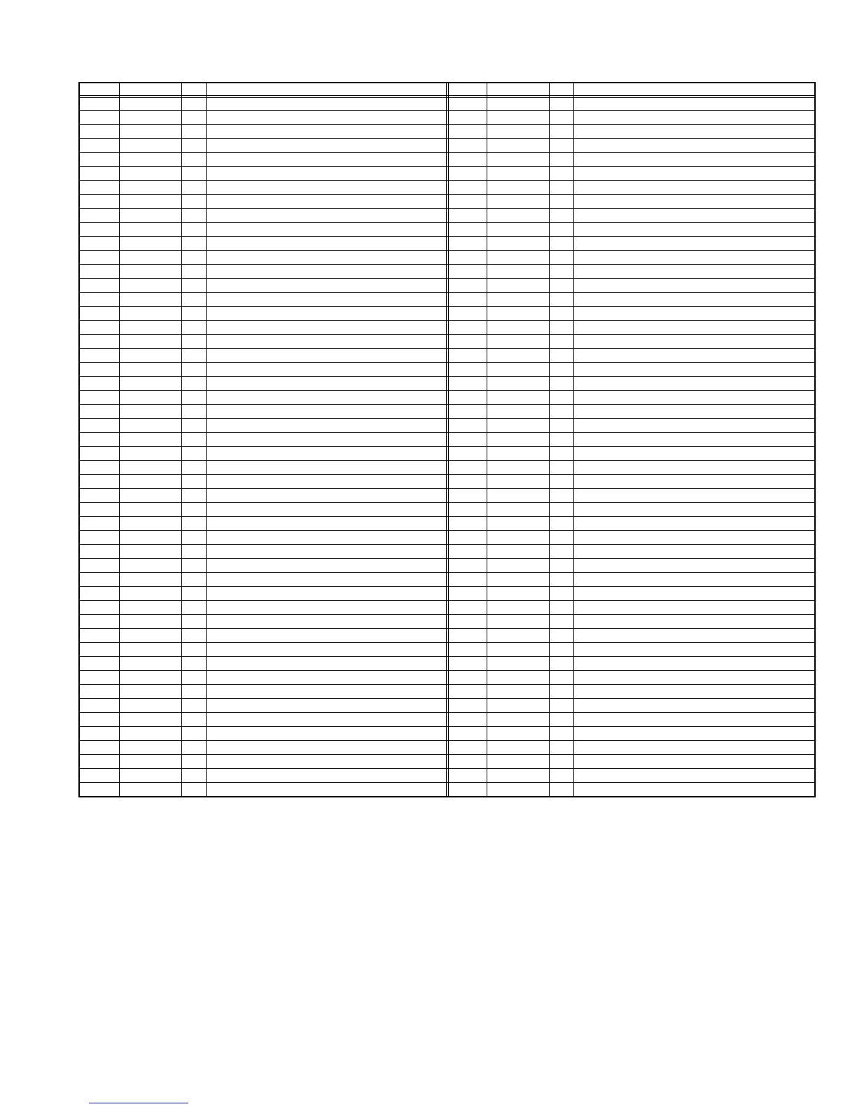
2.4.3 SUB (CHASSIS) CPU PIN FUNCTION [IC7001 : DIGITAL SIGNAL PWB]
Pin Pin name I/O Function Pin Pin name I/O Function
1 LB_PRO O Not used 51 BS_TXD O Not used :
Data transmission for digital tuner communication
2 P_MU O Picture muting [Muting = H] 52 BS_RXD I Not used : Data receive for digital tuner communication
3 JP_CSB O Not used (NC) 53 NC O Not used (NC)
4 A_MU O Audio muting [Muting = H] 54 VREF+ I 3.3V power supply
5 M_MU O Audio muting (for AUDIO OUT) [Muting = H] 55 PDP_TX O
Data transmission for SUB (DRIVE) CPU communication
6 PC_SEL O RGB(PC) INPUT select 56 PDP_RX I Data receive for SUB (DRIVE) CPU communication
7 ON_TIMER O POWER INDICATOR (LED) brightness [LOW = L] 57 SDA0 I/O Data for Inter IC (serial) bus : EEP-ROM (IC7002)
8 ILA0 O LCD back light lighting 58 SCL0 O Clock for Inter IC (serial) bus : EEP-ROM (IC7002)
9 ILA1 O LCD panel overshoot refresh timing 59 SDA_DVI I/O
Not used : Data for Inter IC (serial) bus for panel communication
10 ILA2 O Not used 60 SCL_DVI O
Not used : Clock for Inter IC (serial) bus for panel communication
11 POW_LED O POWER LED lighting [ON = H] 61 AVSS - GND
12 WORD O Not used 62 DIGII_PHOT I Photo sensor for DIGITAL-IN illegal copy protection
13 MI_CK I Clock for main CPU communication 63 AGC I Not used
14 MI_TX I Data receive for main CPU communication 64 EXT_YS1 I Not used
15 MI_RX O Data transmission for MAIN CPU communication 65 EXT_YS2 I Not used
16 MI_REQ O
Data request for main CPU communication [Request = L]
66 VDD I 3.3V power supply
17 VDD I 3.3V power supply 67 DIGI_PRO O Not used : For DIGITAL-IN (HDMI)
18 FOSC O Not used (NC) 68 GCR_RST O Not used (NC)
19 VSS - GND 69 GR_ON O Not used (NC)
20 X1 I Not used : Low speed oscillatior 70 SYNC_SEL O Not used : Sync select for digital tuner
21 X0 O Not used : Low speed oscillatior 71 NC O Not used (NC)
22 VDD I 3.3V power supply 72 NC O Not used (NC)
23 OSC1 I System clock osillation (crystal) : 16MHz 73 SBD5 I/O
Not used : Data for writing on board (connect CN01P : for Frash ROM type)
24 OSC0 O System clock osillation (crystal) : 16MHz 74 SBT5 I
Not used : Clock for writing on board (connect CN01P : for Frash ROM type)
25 MODE I Single chip mode 75 NMI I 3.3V power supply
26 BS1.5CTL O Not used : Digital tuner power / reset control 76 COMP I Not used : AV COMPULINK lll control
27 A92RES O
Reset for IC1001(3D YC SEP / COLOUR DEMODULAT) [Reset = H]
77 REMO I Remote control
28 BS_RST O Not used : Reset for Digital tuner power / reset control 78 VSYNC I V. sync pulse
29 LIP_RST O Not used : Reset for Sound delay (Lip sync) 79 WAKE I Reset for sub(chassis) CPU
30 SOFT_OFF O Not used 80
POWERGOOD
I Power error detection [NG = H]
31 VMUTE I Picture muting request from digital tuner 81 NC O Not used (NC)
32 VOUTENB O Not used : Video cutoff for digital tuner 82 RST I Reset for MAIN CPU [Reset = L]
33 MDR_CON I Not used: System cable connection monitor for PDP 83 VDD I 3.3V power supply
34 AVDD I 3.3V power supply 84 SCL3A O Clock for Inter IC (serial) bus control
35 BS_POW O Not used : Digital tuner power control 85 SDA3A I/O Data for Inter IC (serial) bus control
36
DsyncSW2
O Sync select for DIGITAL-IN [Cotrolled with 99-pin] 86 SCL3B O Clock for Inter IC (serial) bus control
37 LB_POW O Power control for low bias line 87 SDA3B I/O Data for Inter IC (serial) bus control
38 NC O Not used (NC) 88
DIGI_SYNCSEL
O Not used
39 HOTPLUG I
Not used : Video communiation monitor for receiver unit (PDP)
89 DIGI_LRSW O Not used : For DIGITAL-IN (HDMI)
40 MECA_SW I Mechanical monitor for POWER switch [Push = L] 90 DIGI_INT I Reset for HDMI process [Reset = L ]
41 MAIN_POW O Main power control [ON = L] 91 DVI_RST O Not used : Reset for DVI format conversion
42 MSP_RST O AUDIO OUT output mode select [VARIABLE = L] 92 VSS - GND
43 VREF- I Not used 93 SCL5055 O
Clock for Inter IC (serial) bus : JCC5055 (DIST process)
44 AFT2 I Not used : AFT voltage for sub tuner 94
VFORMATSEL
O Not used : Digital tuner clock control
45 AFT1 I AFT voltage for VHF/UHF tuner 95 SDA5055 I/O Data for Inter IC (serial) bus : JCC5055 (DIST process)
46 KEY2 I Key scan data for front switch (MENU/CH+/CH-) 96
OSD_MODE_SEL
O Not used : OSD mode select
47 KEY1 I Key scan data for front switch (VOL+/VOL-) 97 NC O Not used (NC)
48 NC O Not used (NC) 98 15K/OTH O Main video select [Fixed = H]
49 NC O Not used (NC) 99 DsyncSW1 O Sync select for DIGITAL-IN [Cotrolled with 36-pin]
50 AC_IN I Not used : AC 50/60Hz detect 100 57 BUSY I Busy monitor for IC4001 (New DIST process)
 Loading...