Parameter
5 1
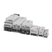
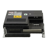
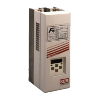
KEB COMBIVERT F5-G / B
12
Name: Basis
14.06.02
Chapter Section Page Date
© KEB Antriebstechnik, 2002
All Rights reserved
Parameter Adr. Control Properties min. max. Step default [?] see on Page
ru 10 encoder 2 speed 020A - - G - - - R - - V -32000 32000 1 0 rpm 6.1.7
ru 13 actual utilization 020D B g G M S A R - - - 0 65535 1 0 % 6.11.6, 6.1.8
ru 14 peak utilization 020E B g G M S A - - - - 0 65535 1 0 % 6.1.8
ru 15 apparent current 020F B g G M S A R - - - 0 6553,5 0,1 0 A 6.1.8
ru 16 peak apparent current 0210 B g G M S A - - - - 0 6553,5 0,1 0 A 6.1.8
ru 17 active current 0211 B g G M S A R - - - -3276,7 3276,7 0,1 0 A 6.12.6, 6.1.9
ru 18 actual DC voltage 0212 B g G M S A R - - - 0 1000 1 0 V 6.12.6, 6.1.9
ru 19 peak DC voltage 0213 B g G M S A - - - - 0 1000 1 0 V 6.1.9
ru 20 output voltage 0214 B g G M S A R - - - 0 778 1 0 V 6.1.9
ru 21 input terminal state 0215 B g G M S A R - - - 0 4095 1 0 - 6.1.10, 6.3.5
ru 22 internal input state 02 16 B g G M S A R - - - 0 4095 1 0 - 6.1.10, 6.3.8
ru 23 output condition state 02 17 B g G M S A R - - - 0 255 1 0 - 6.1.11
ru 24 state of output flags 0218 B g G M S A R - - - 0 255 1 0 - 6.1.11
ru 25 output terminal state 0219 B g G M S A R - - - 0 255 1 0 - 6.1.12, 6.3.18
ru 26 active parameter set 021A B g G M S A R - - - 0 7 1 0 - 6.1.12
ru 27 AN1 pre amplifier disp. 021B B g G M S A R - - - -100,0 100,0 0,1 0 % 6.1.12, 6.2.3, 6.4.4
ru 28 AN1 post amplifier disp. 021C B g G M S A R - - - -400,0 400,0 0,1 0 % 6.1.12, 6.2.3, 6.4.4
ru 29 AN2 pre amplifier disp. 021D - g G M S - R - - - -100,0 100,0 0,1 0 % 6.1.13, 6.2.3, 6.4.4
ru 30 AN2 post amplifier disp. 021E - g G M S - R - - - -400,0 400,0 0,1 0 % 6.1.13, 6.2.3, 6.4.4
ru 31 AN3 pre amplifier disp. 021F - - G M S - R - - - -100,0 100,0 0,1 0 % 6.1.13, 6.2.3, 6.4.4
ru 32 AN3 post amplifier disp. 0220 - - G M S - R - - - -400,0 400,0 0,1 0 % 6.1.13, 6.2.3, 6.4.4
ru 33 ANOUT1 pre ampl. disp. 0221 B g G M S A R - - - -400,0 400,0 0,1 0 % 6.1.14, 6.2.12
ru 34 ANOUT1 post ampl. disp. 0222 B g G M S A R - - - -115,0 115,0 0,1 0 % 6.1.14, 6.2.12
ru 35 ANOUT2 pre ampl. disp. 0223 - g G M S - R - - - -400,0 400,0 0,1 0 % 6.1.14, 6.2.12
ru 36 ANOUT2 post ampl. disp. 0224 - - G M S - R - - - -115,0 115,0 0,1 0 % 6.1.14, 6.2.12
ru 37 motorpoti actual value 0225 B g G M S A R - - - -100,00 100,00 0,01 0 % 6.1.14, 6.9.8
ru 38 power module temperature 0226 B g G M S A R - - - 0 150 1 0 °C 6.1.15
ru 39 OL counter display 02 27 B g G M S A R - - - 0 100 1 0 % 6.1.15
ru 40 power on counter 0228 B g G M S A R - - - 0 65535 1 0 h 6.1.15
ru 41 modulation on counter 0229 B g G M S A R - - - 0 65535 1 0 h 6.1.15
ru 42 modulation grade 022A B g G M S A R - - - 0 110 1 0 % 6.1.15
ru 43 timer 1 display 022B B g G M S A - - - - 0 655,35 0,01 0 - 6.1.15, 6.9.12
ru 44 timer 2 display 022C B g G M S A - - - - 0 655,35 0,01 0 - 6.1.16, 6.9.12
ru 45 act. carrier frequency 022D B g G M S A R - - - 0 4 1 0 - 6.1.16
ru 46 motor temperature 022E B g G M S - R - - - 0 255 1 0 °C 6.1.16
ru 52 ext. PID out disp. 0234 B g G M S A R - - - -100,0 100,0 0,1 0 % 6.1.17, 6.4.4
ru 53 AUX display 02 35 B g G M S A R - - - -400,0 400,0 0,1 0 % 6.1.17, 6.12.6
ru 68 rated DC voltage 0244 B g G M S A R - - - 0 1000 1 0 V
sy 2 inverter identifier 0002 B g G M S A - - - - identifier identifier 1 identifier hex 6.1.23
sy 3 power unit code 0003 B g G M S A - - E - 1 255 1 LTK - 6.1.23
sy 6 inverter address 0006 B g G M S A - - E - 0 239 1 1 - 6.1.23, 11.2.3
sy 7 baud rate ext. bus 0007 B g G M S A - - E - 0 6 1 5 - 6.1.23, 11.2.3
sy 9 HSP5 watchdog time 0009 B g G M S A - - E - 0,00:off 10,00 0,01 0,00:off s 6.1.24, 11.2.3
sy11 baud rate int. bus 000B B g G M S A - - E - 3 11 1 5 - 6.1.24, 11.2.3
sy32 scope timer 0020 B g G M S A R - - - 0 65535 1 0 - 6.1.24
sy41 control word (high) 00 29 - - G M S A - - E - 0 65535 1 0 hex 6.1.24, 11.2.4
sy42 status word (high) 002A - - G M S A R - - - 0 65535 1 0 hex 6.1.25, 11.2.5
sy43 control word (long) 002B - - G M S A - - E - -2^31 2^31 - 1 1 0 hex 6.1.25, 11.2.4
sy44 status word (long) 002C - - G M S A R - - - -2^31 2^31 - 1 1 0 hex 6.1.25, 11.2.5
sy50 control word (low) 0032 B g G M S A - - E - 0 65535 1 0 hex 6.1.25, 6.4.8, 11.2.4
sy51 status word (low) 0033 B g G M S A R - - - 0 65535 1 0 hex 6.1.25, 11.2.4
sy52 set speed value 0034 B g G M S A - - - - -16000 16000 1 0 rpm 6.1.26, 11.2.4
sy53 actual speed value 0035 B g G M S A R - - - -16000 16000 1 0 rpm 6.1.25, 11.2.4
sy56 start display address 0038 B g G - - A - - E - 0 7FFFH 1 0203H hex 6.1.25
ud 1 password 0801 B g G M S A - - - - 0 9999 1 application - 4.2.3, 4.4.3, 6.13.3
ud 2 maximum frequency mode 0802 B g - -------0 2 1 0 - 6.5.3
ud 2 control type 08 02 - - G M S A - - E - 0 10 1 0 - 6.5.3
ud 5 auto store 0805 B g - -------0 1 1 1 -
ud 9 drive-mode-control 08 09 B g G M S A - - - - 0 11 1 0 - 4.4.4
ud15 cp selector 080F B g G M S A - - E - 1 36 1 1 - 6.13.4
ud16 cp address 0810 B g G M S A - - E - -1 32767 1 Tabelle hex 6.13.4
ud17 cp set norm 08 11 B g G M S A - - E - 1 32767 1 1 - 6.13.4
ud18 divisor display norm 0812 B g G M S A - P E - -32767 32767 1 1 - 6.13.6
ud19 multiplier display norm 0813 B g G M S A - P E - -32767 32767 1 1 - 6.13.6
ud20 offset display norm 0814 B g G M S A - P E - -32767 32767 1 0 - 6.13.6
ud21 ctrl. display norm 0815 B g G M S A - P E - 0 1791 1 0 - 6.13.6
uf 0 rated frequency 0500 B g G M - A - P - V 0 400 0,0125 50 Hz 6.5.4
uf 1 boost 0501 B g G M - A - P - - 0,0 25,5 0,1 2,0 % 6.5.4
uf 2 add. frequency 05 02 B g G M - A - P - V -0,0125 400 0,0125 0:off Hz 6.5.4
uf 3 add. voltage 0503 B g G M - A - P - - 0,0 100,0 0,1 0,0 % 6.5.4
uf 4 delta boost 0504 B g G M - A - P - - 0,0 25,5 0,1 0,0 % 6.5.4
uf 5 delta boost time 0505 B g G M - A - P - - 0,00 10,00 0,01 0,00 s 6.5.4
uf 6 energy saving mode 0506 B g G M - A - P - - 0 7 1 0 - 6.9.5
uf 7 energy saving factor 0507 B g G M - A - P - - 0,0 130,0 0,1 70,0 % 6.9.5
uf 8 energy saving input sel. 0508 B g G M - A - - E - 0 4095 1 0 - 6.9.5, 6.3.8
uf 9 voltage stabilisation 0509 B g G M - - - P E - 1 650:off 1 650:off V 6.5.5
uf 10 max. voltage mode 050A - - G M - A - P - - 0 3 1 0 - 6.5.6