Troubleshooting
5-7
Both the digital I/O and trigger link circuits have protection
circuits to prevent damage from external circuits. CR603,
CR605, CR607, and CR609 protect the digital I/O circuits,
while the various trigger lines are protected by CR611-
CR618, as well as by CR635-CR639 and CR642.
Power supply circuits
While most power supply circuits are located on the analog
board, several supplies are located on the digital board.
These include the +5V3, +5V, line frequency, and VFD
power supply circuits.
AC voltage from the power transformer is rectified by
CR622 and filtered by C611. U642 regulates the +5V3
supply, and U629 regulates the +5V supply. The square wave
line frequency signals LINEFREQ1 and LINEFREQ2 are
generated by U628 and associated components. The MO-30
power supply module generates the voltages necessary to
operate the VFD located on the display board, while, U643,
U652, and U653 generate the +8VD and -8VD supply
voltages.
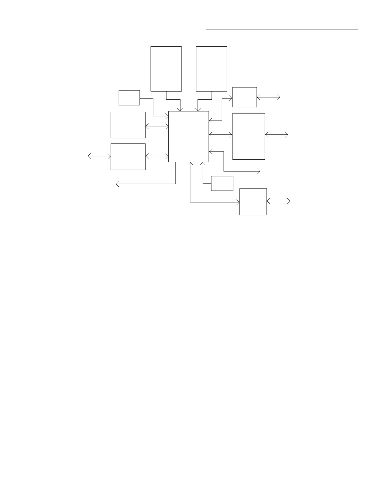
ROM
U637, U638
RAM
U635, U636
NVRAM
U634 - U640
Microprocessor
U631
GPIB
U621 - U623
IEEE - 488 Interface
A/D
Control/Data
A/D Interface
U614
Voltage Source
Control
Reset
U639
Serial
Interface
U641
RS-232 Interface
16MHz
Y602
To Display
Board Controller
Trigger,
Digital I/O
U612,
U618
Trigger/
Digital I/O
Figure 5-4
Digital board block diagram
5.5.4 Analog board
Figure 5-5 is a block diagram of the analog board. Various
sections of the analog board are covered below with the ex-
ception of the power supply circuits, which are covered sep-
arately paragraph 5.5.2.
Input preamplifier
The input preamplifier stage provides the high input imped-
ance necessary for the voltage function, as well as the low
input bias current and current- or charge-to-voltage conver-
sion for the amps, ohms, and coulombs functions. The input
preamplifier is essentially made up of three sections: the
input stage, range/function switching, and the output stage.
The input stage is made up of U405 and associated compo-
nents. This IC has the required low input bias current, and it
also provides the overall gain for the input preamplifier.
The output stage includes Q402-Q413 and associated com-
ponents. This stage supplies the necessary voltage and cur-
rent drive capability for the input preamplifier.