The USB interface consists of the normal bidirectional control endpoint 0 and two bidirectional
bulk endpoints: Endpoint 1 and Endpoint 2. Endpoint 1 consists of a 128 byte OUT endpoint
and a 128 byte IN endpoint. Endpoint 2 consists of a 0 byte OUT endpoint and a 256 byte IN
endpoint. Endpoint 2 OUT is not supported by the firmware, and should never be used.
All commands should always be sent on Endpoint 1, and the responses to commands will also
always be on Endpoint 1. Endpoint 2 is only used to send stream data from the U3 to the host.
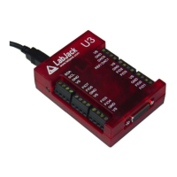
2.2 Status LED
There is a green status LED on the LabJack U3. This LED blinks on reset, and then remains
steadily lit.
2.3 GND and SGND
The GND connections available at the screw-terminals and DB connectors provide a common
ground for all LabJack functions. This ground is the same as the ground line on the USB
connection, which is often the same as ground on the PC chassis and therefore AC mains
ground.
SGND is located on the screw terminal block with SDA and SCL. This terminal has a self-
resetting thermal fuse in series with GND. This is often a good terminal to use when connecting
the ground from another separately powered system that could unknowingly already share a
common ground with the U3.
See the AIN, DAC, and Digital I/O Sections for more information about grounding.
2.4 Vs
The Vs terminals are designed as outputs for the internal supply voltage (nominally 5 volts).
This will be the voltage provided from the USB cable. The Vs connections are outputs, not
inputs. Do not connect a power source to Vs in normal situations. All Vs terminals are the
same.
2.5 Flexible I/O (FIO/EIO)
The first 16 I/O lines (FIO and EIO ports) on the LabJack U3 can be individually configured as
digital input, digital output, or analog input. In addition, up to 2 of these lines can be configured
as timers, and up to 2 of these lines can be configured as counters. If a line is configured as
analog, it is called AINx according to the following table:
AIN0 FIO0 AIN8 EIO0
AIN1 FIO1 AIN9 EIO1
AIN2 FIO2 AIN10 EIO2
AIN3 FIO3 AIN11 EIO3
AIN4 FIO4 AIN12 EIO4
AIN5 FIO5 AIN13 EIO5
AIN6 FIO6 AIN14 EIO6
AIN7 FIO7 AIN15 EIO7
Table 2-1. Analog Input Pin Locations
13