Technical data
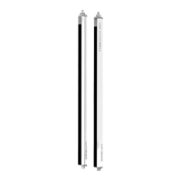
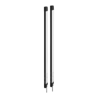
Leuze electronic SOLID-2 47
TNT 35/7-24V
Review-Stand, , 8. April 2015
DEUTSCHENGLISHFRANÇAISITALIANOESPAÑOLNEDERLANDS
10.1.6 Receiver transistor safety switch outputs
OSSDs
transistor safety switch outputs
2 safety pnp transistor outputs, cross-circuit
monitoring, short-circuit-proof
Minimum Typical Maximum
Switching voltage high active
Switching voltage low
Switching current
Leakage current
Load capacity
Load inductivity
Uv - 1,9 V Uv – 1 V
200 mV
< 2 μA*)
Uv - 0,8 V
+ 1 V
250 mA
< 2,2 μF
2,0 H
Permissible wire resistance for load – –
< 50 Ω**
)
Permissible wire cross-section
Receiver Standard
Receiver Extended
0,25 mm² 0,14
mm²
Permissible cable length between
Receiver and load
– – 100 m***)
Auxiliary pulse width 20 μs – 230 μs
Auxiliary pulse spacing 3,7 ms – 46 ms
OSSD restart after beam interruption
w/o RES
– 100 ms –
OSSD response time Depends on the number of beams. See the tables
in Chapter
10.2
*
)
In the event of an error (if the GND line is interrupted) the output behaves like a 120 kΩ to Uv. A
downstream safety interface/PLC must not detect this as a logical “1“.
**) Note the additional restrictions caused by cable length and load current.
***) The specified cable length may be limited by inductive or capacitive loads.
This limitation can eliminated by terminal resistors (2 kΩ) in parallel to each of the loads,
connected between the OSSDS wire ends and 0V (Ground).
• Spark suppression is carried out by the transistor outputs. It is therefore not necessary
to use spark extinguishers recommended by manufacturers of contactors and valves
(RC modules, varistors or recovery diodes) with transistor outputs. These would extend
the delay time of the inductive switching elements.
Table 10.1-6: Receiver, Transistor outputs