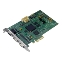
Connectors on Matrox Solios eV-CLB and eV-CLF boards 89
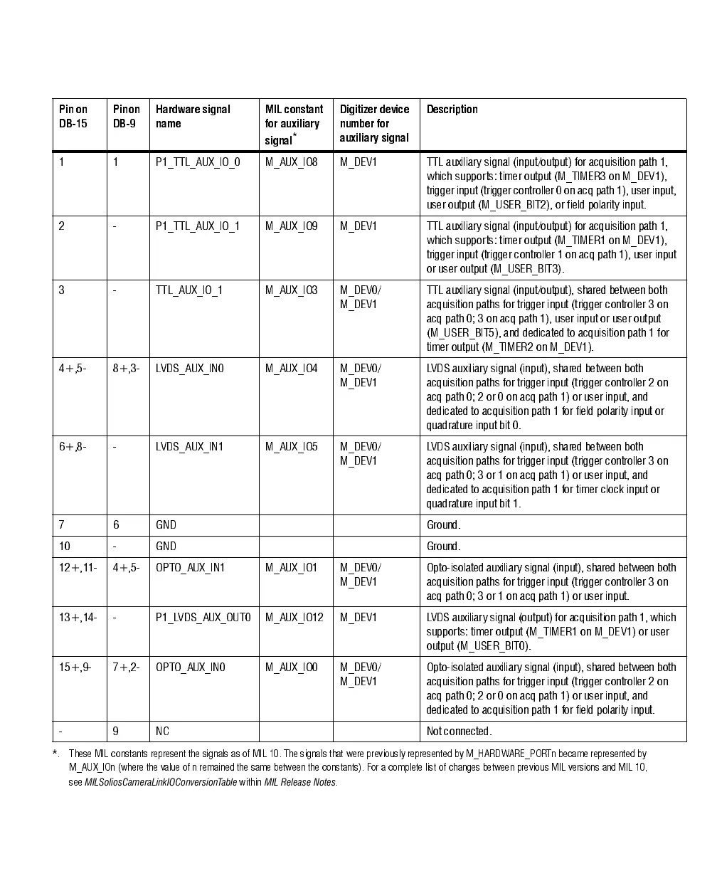
Pin on
DB-15
Pin on
DB-9
Hardware signal
name
MIL constant
for auxiliary
signal
*
Digitizer device
number for
auxilia ry signal
Description
1 1 P1_TTL_AUX_IO_0 M_AUX_IO8 M_DEV1 TTL auxiliary signal (input/output) for acquisition path 1,
which supports: timer output (M_TIMER3 on M_DEV1),
trigge r in put (tri gge r controller 0 on acq path 1), user i nput,
user output (M_USER_BIT2), or field polarity input.
2 - P1_TTL_AUX_IO_1 M_AUX_IO9 M_DEV1 TTL auxiliary signal (input/output) for acquisition path 1,
which supports: timer output (M_TIMER1 on M_DEV1),
trigger input (trigger controller 1 on acq path 1), u ser input
or user output (M _USER_BIT 3).
3 - TTL_AUX_IO_1 M_AUX_IO3 M_DEV0/
M_DEV1
TTL auxiliary signal (input/output), shared between both
acquisition paths for trigger inpu t (trigger controller 3 on
acq path 0; 3 on acq path 1), user input or user output
(M_USER_BIT5), and dedicated to acquisition path 1 for
timer output (M_TIMER2 on M_DEV1).
4+,5- 8+,3- LVDS_AUX_IN0 M_AUX_IO4 M_DEV0/
M_DEV1
LVDS auxiliary signal (input), shared between both
acquisition paths for trigger inpu t (trigger controller 2 on
acq path 0; 2 or 0 on acq path 1) or user input, and
dedicated to acquisition path 1 for fie ld polarity input or
quadrature in put bit 0.
6+,8- - LVDS_AUX_IN1 M_AUX_IO5 M_DEV0/
M_DEV1
LVDS auxiliary signal (input), shared between both
acquisition paths for trigger inpu t (trigger controller 3 on
acq path 0; 3 or 1 on acq path 1) or user input, and
dedicated to acquisition path 1 for timer clock input or
quadrature in put bit 1.
7 6 GND Ground.
10 - GND G round.
12+,11- 4+,5- OPTO_AUX_IN1 M_AUX_IO1 M_DEV0/
M_DEV1
Opto-isolated auxiliary signal (input), shared betwee n both
acquisition paths for trigger inpu t (trigger controller 3 on
acq path 0; 3 or 1 on acq path 1) or user input.
13+,14- - P1_LVDS_AUX_OUT0 M_ AUX_IO12 M_DEV1 LVDS a uxiliary signal (output) for acquisi tion path 1, which
supports: timer output (M_TIMER 1 on M_DEV1 ) or user
output (M_USER_BIT0 ).
15+,9- 7+,2- OPTO_AUX_IN0 M_AUX_IO0 M_DEV0/
M_DEV1
Opto-isolated auxiliary signal (input), shared betwee n both
acquisition paths for trigger inpu t (trigger controller 2 on
acq path 0; 2 or 0 on acq path 1) or user input, and
dedicated to acquisition path 1 for fie ld polarity input.
- 9 NC Not connected.
*. These MIL constants represent the signals as of MIL 10. The signals that were previously represented by M_HARDWARE_PORTn became re presented by
M_AUX_IOn (where the value of n remained the same between the constants). For a complete list of changes between previous MIL versions and MIL 10,
see
MILSoliosCameraLinkIOConversionTable
within
MIL Release Notes
.