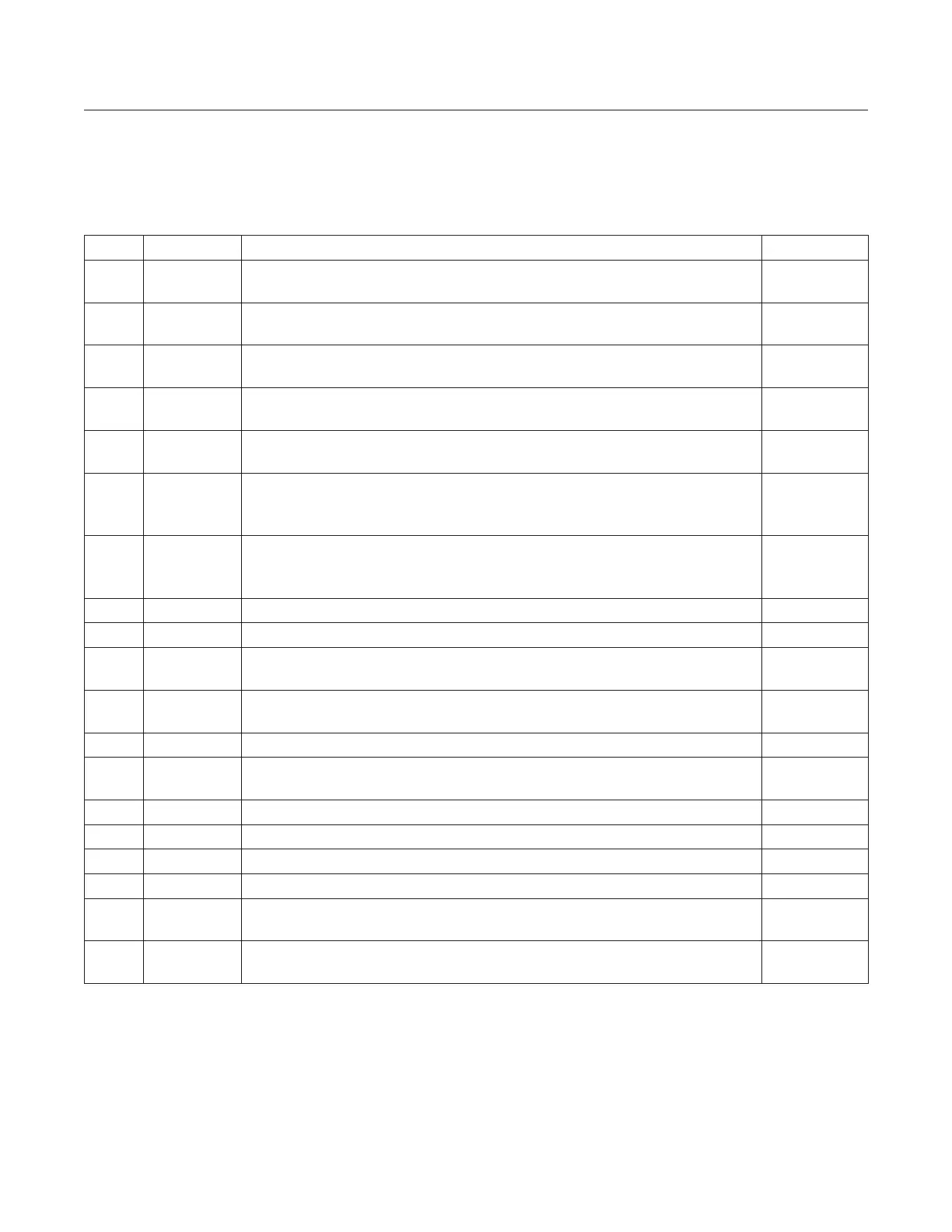
PIN NAME FUNCTION TYPE
10 Q1
Q-Channel Voltage Outputs. Bits 0 and 1 of the Q-channel ADC output or analog
dierential voltage output.
Digital or
analog output
11 Q0
Q-Channel Voltage Outputs. Bits 0 and 1 of the Q-channel ADC output or analog
dierential voltage output.
Digital or
analog output
12 I0
I-Channel Voltage Outputs. Bits 0 and 1 of the I-channel ADC output or analog
dierential voltage output.
Digital or
analog output
13 I1
I-Channel Voltage Outputs. Bits 0 and 1 of the I-channel ADC output or analog
dierential voltage output.
Digital or
analog output
14 VCCADC
ADC Supply Voltage. Bypass to ground with a 100nF capacitor as close as
possible to the pin.
Power
15 ANAIPOUT
The Analog I+ Channel is Output On This Pin. This is used for the continuous
spectrum monitoring function if the ANAIMON bit is set to 1. If continuous spectrum
monitoring feature is not required, leave unconnected.
Analog output
16 ANAINOUT
The Analog I- Channel is Output On This Pin. This is used for the continuous spectrum
monitoring function if the ANAIMON bit is set to 1. If continuous spectrum monitoring
feature is not required, leave unconnected.
Analog output
17 LD Lock-Detector CMOS Logic Output. A logic-high indicates the PLL is locked. Digital output
18 SHDN Operation Control Logic Input. A logic-low shuts o the entire device. Digital input
19 LNAIN_HI
High-Band LNA Input Port. Requires external matching circuit of 5.6nH series
inductor and 1.7pF shunt capacitor.
Analog input
20 LNAIN_LO
Low-Band LNA Input Port. Requires external matching circuit of 8.4nH series
inductor and 1.1pF shunt capacitor.
Analog input
21 NC No Connection. Leave this pin unconnected.
22 VCCRF
RF Section Supply Voltage. Bypass to ground with 100nF and 100pF capacitors in
parallel as close as possible to the pin.
Power
23 LNAOUT_LO Low-Band LNA Output. The LNA output is internally matched to 50Ω for L2/L5 band. Analog output
24 LNAOUT_HI High-Band LNA Output. The LNA output is internally matched to 50Ω for L1 band. Analog output
25 MIXIN_HI High-Band Mixer Input. The mixer input is internally matched to 50Ω for L1 band. Analog input
26 MIXIN_LO Low-Band Mixer Input. The mixer input is internally matched to 50Ω for L2/L5 band. Analog input
27 VCCIF
IF Section Supply Voltage. Bypass to ground with a 100nF capacitor as close as
possible to the pin.
Power
28 VCCVCO
VCO Supply Voltage. Bypass to ground with a 100nF capacitor as close as possible
to the pin.
Power
Pin Description (continued)
www.maximintegrated.com
Maxim Integrated
│
15
MAX2771 Multiband Universal GNSS Receiver