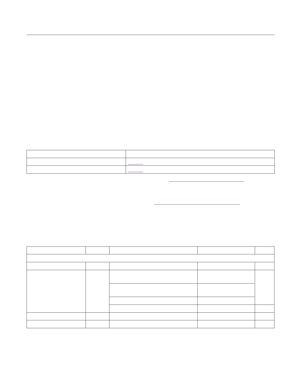
VCC to GND ......................................................... -0.3V to +4.2V
MIXIN_ to GND ....................................................-0.3V to +0.3V
Other Pins to GND (Note 1) ........................-0.3V to V
CC
+ 0.3V
Maximum RF Input Power ..............................................+15dBm
Continuous Power Dissipation
(T
A
= +70°C, derate 27 mW/°C above +70°C.) ........2500mW
Operating Temperature Range ..............................-40°C to 85°C
Storage Temperature Range ............................ -65°C to +150°C
Junction Temperature ...................................................... +150°C
Lead Temperature (Soldering, 10 seconds) .................... +300°C
(MAX2771 EV kit, V
CC
= 2.7V to 3.3V, T
A
= -40°C to +85°C. Registers are set to the specified default states. LNA input is driven from
a 50Ω source. All RF measurements are done in the analog output mode with ADC bypassed. PGA gain is set to GAININ = 111010
through SPI interface, unless otherwise noted. Maximum IF output load is not to exceed 10kΩ||7.5pF on each pin. Typical values are
at V
CC
= 2.85V and T
A
= +25°C, unless otherwise noted. (Note 1))
Note 1: Except for LNAIN_HI, LNAIN_LO, MIXIN_HI, MIXIN_LO, XTAL, LNAOUT_HI and LNAOUT_LO
Idle Mode is a trademark of Maxim Integrated Products, Inc.
PARAMETER SYMBOL CONDITIONS MIN TYP MAX UNITS
DC ELECTRICAL CHARACTERISTICS
Supply Voltage VCC 2.7 2.85 3.3 V
Supply Current
Default mode, high-band LNA and mixer
input is active (Note 2)
26
mA
Default mode, low-band LNA and mixer input
is active (Note 2)
27
Idle Mode
TM
, IDLE bit is 1, SHDN = high
5
Shutdown mode, SHDN= low
200 μA
Digital Input Logic-High V
IH
Measure at the SHDN pin
1.5 V
Digital Input Logic-Low V
IL
Measure at SHDN pin
0.4 V
Package Code T2855+8
Outline Number 21-0140
Land Pattern Number 90-0023
Absolute Maximum Ratings
Stresses beyond those listed under “Absolute Maximum Ratings” may cause permanent damage to the device. These are stress ratings only, and functional operation of the device at these
or any other conditions beyond those indicated in the operational sections of the specifications is not implied. Exposure to absolute maximum rating conditions for extended periods may affect
device reliability.
Package thermal resistances were obtained using the method described in JEDEC specification JESD51-7, using a four-layer board.
For detailed information on package thermal considerations, refer to www.maximintegrated.com/thermal-tutorial.
For the latest package outline information and land patterns (footprints), go to www.maximintegrated.com/packages. Note that a “+”,
“#”, or “-” in the package code indicates RoHS status only. Package drawings may show a different suffix character, but the drawing
pertains to the package regardless of RoHS status.
Package Information
28 TQFN-EP
Electrical Characteristics
www.maximintegrated.com
Maxim Integrated
│
6
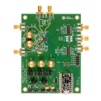
MAX2771 Multiband Universal GNSS Receiver