Table 1. Required Register Bit Field Values ........................................................ 17
Table 2. Default Register Setting ................................................................. 17
Table 3. LNA Selection ........................................................................ 17
Table 4. Mixer Selection........................................................................ 18
Table 5. IF Filter Mode Selection ................................................................. 18
Table 6. IF Filter Order Selection................................................................. 19
Table 7. IF Filter Bandwidth Selection ............................................................. 19
Table 8. Gain Reference Settings ................................................................ 19
Table 12. Output Data Format ................................................................... 20
Table 9. ADC Output Data Format Settings......................................................... 20
Table 10. IQ Channels Enable Settings ............................................................ 20
Table 11. ADC Output Bits Setting................................................................ 20
Table 13. Frequency of ADC Sampling Clock vs. Reference Clock ...................................... 22
Table 14. Reference Divider Settings.............................................................. 25
Table 15. Serial Interface Timing Requirements ..................................................... 27
Table 16. External Component List ............................................................... 49
LIST OF TABLES
www.maximintegrated.com
Maxim Integrated
│
5
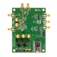
MAX2771 Multiband Universal GNSS Receiver