Table 15. Serial Interface Timing Requirements
SYMBOL PARAMETER MIN MAX UNITS
t
CSS
Falling edge of CSN to rising edge of the rst SCLK pulse 10 ns
t
DS
Data in to SCLK setup time 10 ns
t
DH
Data in to SCLK hold time 10 ns
t
CP
SCLK period 250 ns
t
DAZ
SCLK falling edge to SDATA tri-stated 25 ns
t
DZA
SCLK falling edge to SDATA active 25 ns
t
CSH
Last SCLK rising edge to rising edge of CSN 10 ns
t
DP
SCLK falling edge to data out propagation delay 25 ns
t
CSNOFF
CSN rising edge to next SPI transaction CSN falling edge 100 ns
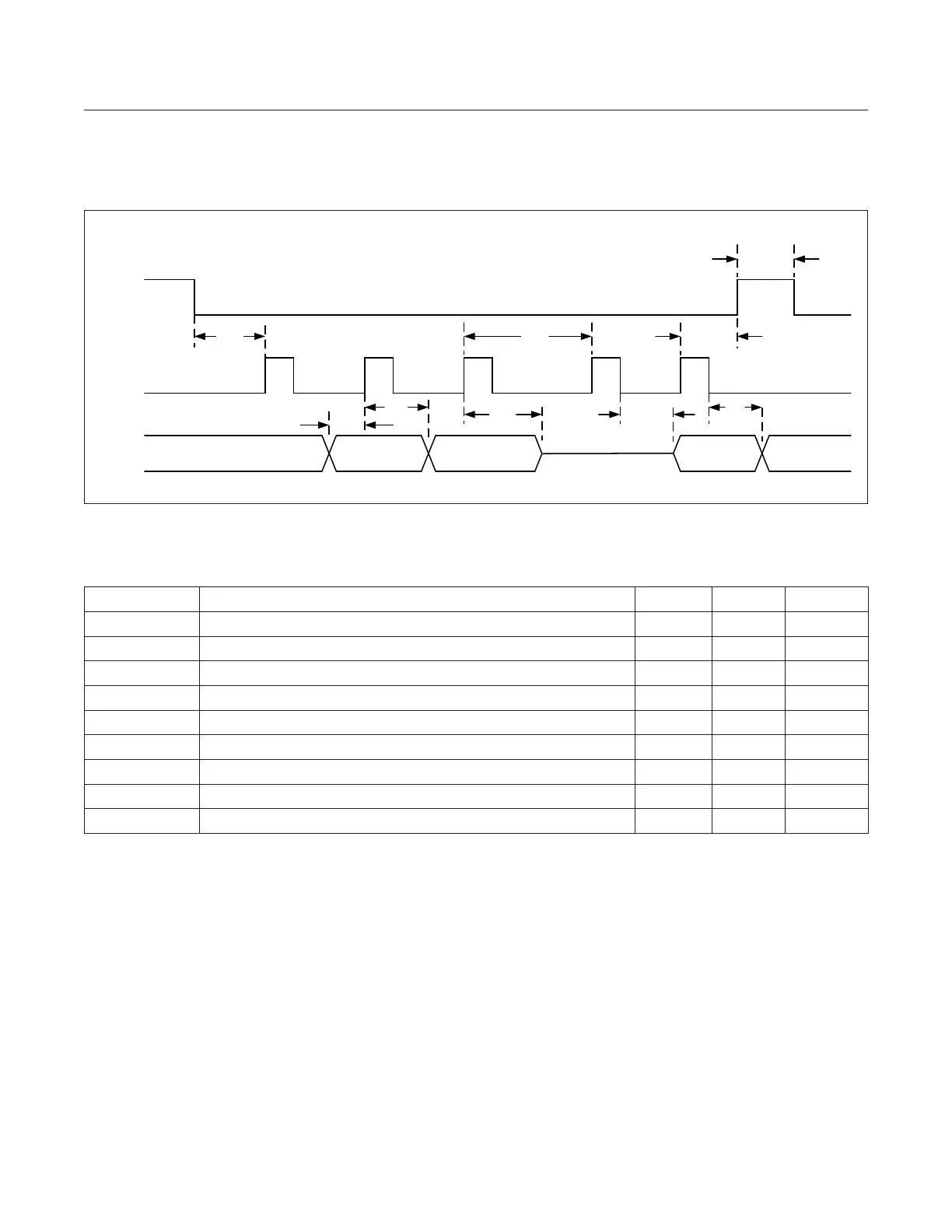
Figure 6. Three-Wire Interface Timing Diagram
SCLK
CSN
SDATA
t
DS
t
CP
t
CSS
t
CSH
t
DH
t
DAZ
t
DZA
t
DP
t
C SNOFF
www.maximintegrated.com
Maxim Integrated
│
27
MAX2771 Multiband Universal GNSS Receiver