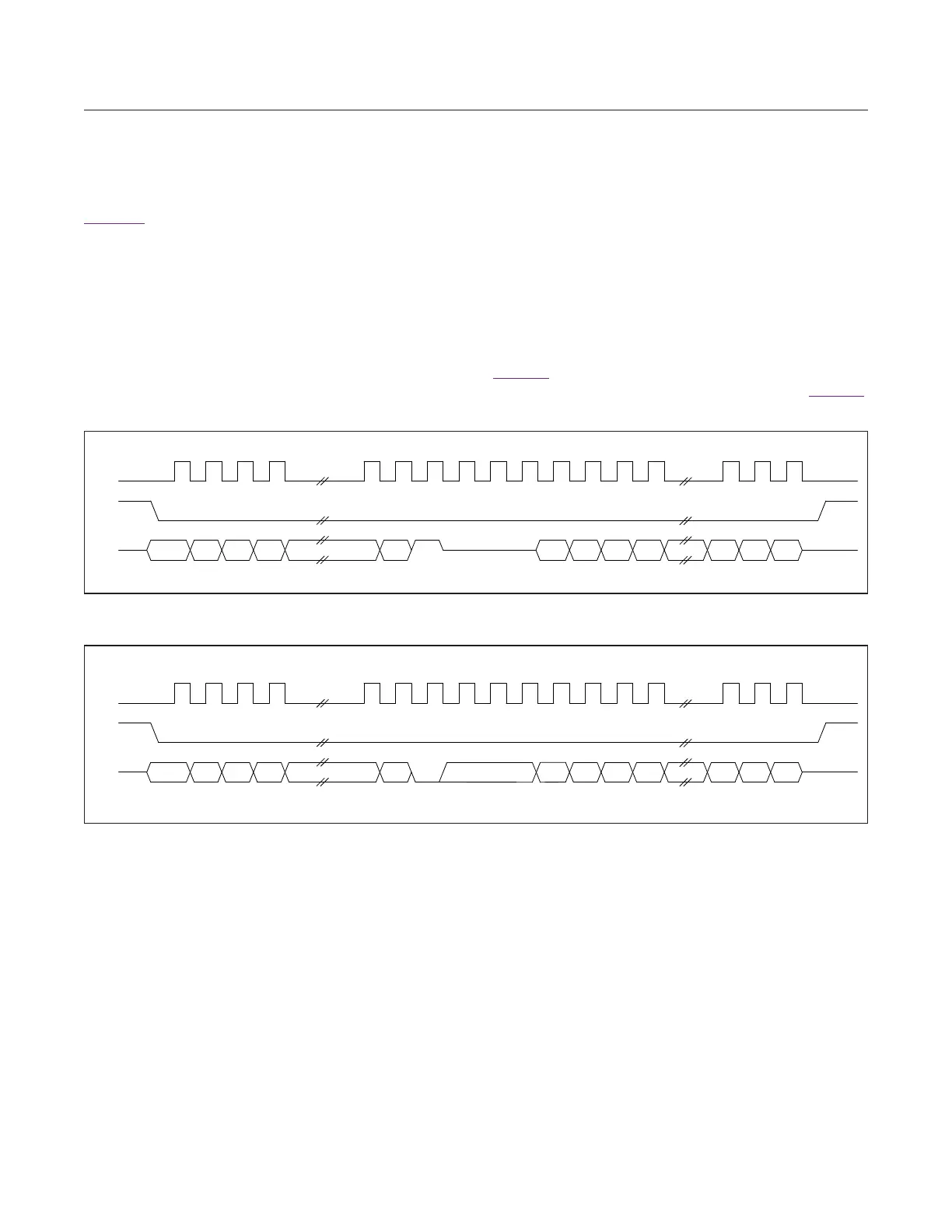
Figure 5 shows a register write transaction. In this
example, a 32-bit register is written by the host. The
host first asserts CSN, begins driving SDATA with the
register address preceded by 8 zeros and starts toggling
SCLK. The MAX2771 samples the bits on SDATA on the
rising edge of SCLK. After the address is output, the host
outputs a R/W bit having value of 0 indicating this a write
transaction. The next bits are the TA bits. Since this is a
write, the host may choose to continue driving SDATA
during this interval. The next 32 SCLKs, the host outputs
the 32-bit data to be written to the addressed register
starting from the most significant bit. After the last bit has
been output, the host tri-states SDATA, and subsequently
brings CSN high completing the transaction.
If the host does not assert CSN, the MAX2771 will
ignore any activity on SCLK or SDATA. This allows multiple
MAX2771 devices to be connected to the SPI and
controlled by one host. Only the MAX2771 that has its
CSN input asserted will react to the host.
Figure 6 illustrates the timing relationships between the
three signals of the three-wire interface. Refer to Table 15.
Figure 4. Register Read Functional Timing
Figure 5. Register Write Functional Timing
SCLK
CSN
SDIO
HI-Z
A11
0 1 2 3 10 11 12 13 14 15 16 17 18 19 45 46 47
A10 A9 A8 A0 R/W
TA
D31 D30 D29 D28 D2 D1 D0
HI-Z
SCLK
CSN
SDIO
HI-Z
A11
0 1 2 3 10 11 12 13 14 15 16 17 18 19 45 46 47
A10 A9 A8 A0 R/W
TA
D31 D30 D29 D28 D2 D1 D0
HI-Z
www.maximintegrated.com
Maxim Integrated
│
26
MAX2771 Multiband Universal GNSS Receiver