PIN NAME FUNCTION TYPE
1 CPOUT
Charge-Pump Output. Connect a PLL loop lter as a shunt C and a shunt combination
of series R and C (see Typical Application Circuit).
Analog output
2 VCCCP
PLL Charge-Pump Supply Voltage. Bypass to ground with a 100nF capacitor as close
as possible to the pin.
Power
3 XTAL
XTAL or Reference Oscillator Input. Connect to XTAL or a DC-blocking capacitor if a
TCXO is used.
Analog input
4 CLKOUT Reference Clock Output. Digital output
5 ADC_CLKIN
ADC Clock Input. Optionally, the ADCs can be clocked from the clock input on this pin.
Refer to ADC Clock Alignment section for details.
Digital input
6 VCCD
Digital Circuitry Supply Voltage. Bypass to ground with a 100nF capacitor as close as
possible to the pin.
Power
7
SDATA Data Signal of 3-Wire Serial Interface.
Digital Input/
Output
8 SCLK
Clock Input of 3-Wire Serial Interface. Serial data is clocked in on the rising-edge of
the SCLK and output on the falling-edge of SCLK.
Digital Input
9 CSN
Chip-Select Input of 3-Wire Serial Interface. Set CSN low to select device.
Set CS high when the SPI transaction is completed.
Digital Input
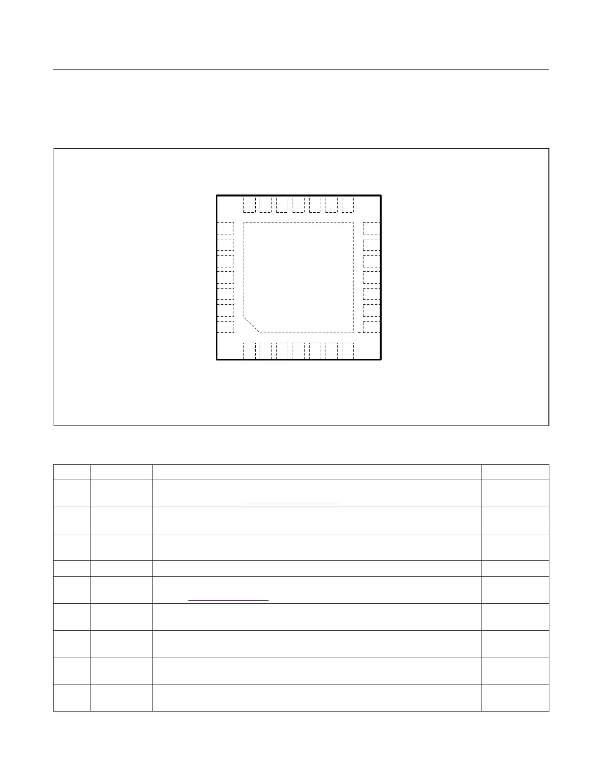
Pin Conguration
21 20 19 18 17 16 15
+
EP
TOP VIEW
MAX2771
N.C.
LNAIN_LO
LNAIN_HI
SHDN
LD
ANAINOUT
ANAIPOUT
VCCRF
LNAOUT_LO
LNAOUT_HI
MIXIN_HI
MIXIN_LO
VCCIF
22
23
24
25
26
27
VCCVCO
28
14
13
12
11
10
9
VCCADC
I1
I0
Q0
Q1
CSN
8 SCLK
1 2 3 4 5 6 7
CPOUT
VCCCP
XTAL
CLKOUT
ADC_CLKIN
VCCD
SDATA
*CONNECTED EXPOSED PAD TO GROUND
Pin Description
www.maximintegrated.com
Maxim Integrated
│
14
MAX2771 Multiband Universal GNSS Receiver