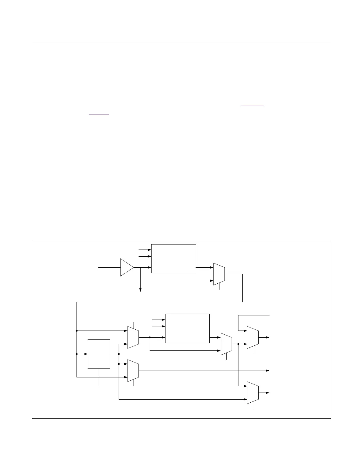
Reference Clock
The crystal clock input on pin 3 is used to generate
internal clocks and a reference clock that is output to
the baseband. The block diagram illustrating the clock
distribution is shown in Figure 3. There is a 12-bit fractional
pre-divider that optionally allows division of the XTAL
clock by some fractional amount. In the fractional divider
mode, the instantaneous division ratio alternates between
integer division ratios to achieve the required fraction. For
example, if the fractional output clock is 4.5 times lower
frequency than the input clock, an average division ratio
of 4.5 is achieved through an equal series of alternating
divide-by-4 and divide-by-5 periods. The fractional
division ratio is given by:
f
OUT
/f
IN
= LCOUNT/(4096 - MCOUNT + LCOUNT)
where LCOUNT and MCOUNT are the 12-bit counter
values in the Clock Configuration 1 register. The frac-
tional division ratio cannot exceed 0.5. This divider can be
enabled or bypassed by setting the PREFRACDIV_SEL
bit in the Clock Configuration 2 register to either 0 or 1.
The reference clock can then be optionally divided by
either two or four, or multiplied by two or four. This is
determined by the REFCLK bits in the PLL Configuration
Register. Refer to Table 14. This table ignores the
fractional ratio. The maximum frequency of the pre-divided
reference clock is 22MHz if the x2 option is selected,
and 11MHz if the x4 option is selected. The ADC
sampling clock can then be generated by a second fractional
divider. This is described in the section on the ADC. The
CLKOUT signal to the baseband can be selected to either
be the output of the integer divider/multiplier block or the
ADC clock. This selection is done through the CLKOUT_
SEL bit in the Clock Configuration 2 register.
The ADC clock can either be selected to be the
internally generated clock, or taken from outside the
IC. The EXTADCLK register bit selects whether the
ADCs are clocked from the internally generated clock,
or use the clock provided on the ADC_CLKIN pin. This
feature allows multiple MAX2771 devices connected to a
common baseband IC to have synchronized ADC outputs.
The maximum clock frequency for any of these clocks is
44MHz.
Figure 3. Clock Distribution
XTAL
PIN 3
TO PLL
PREFRACDIV_SEL
L_CNT[11:0]
M_CNT[11:0]
CLK_IN CLK_OUT
THRU
/2
/4
X2
X4
REFDIV[2:0]
ADCCLK_SEL
SERCLK_SEL
FRCLK_SEL
ADC_CLKIN
PIN 5
CLK_ADC
EXTADCCLK
CLK_SER
CLK_OUT
PIN 4
CLKOUT_SEL
L_CNT[11:0]
M_CNT[11:0]
CLK_IN CLK_OUT
www.maximintegrated.com
Maxim Integrated
│
24
MAX2771 Multiband Universal GNSS Receiver