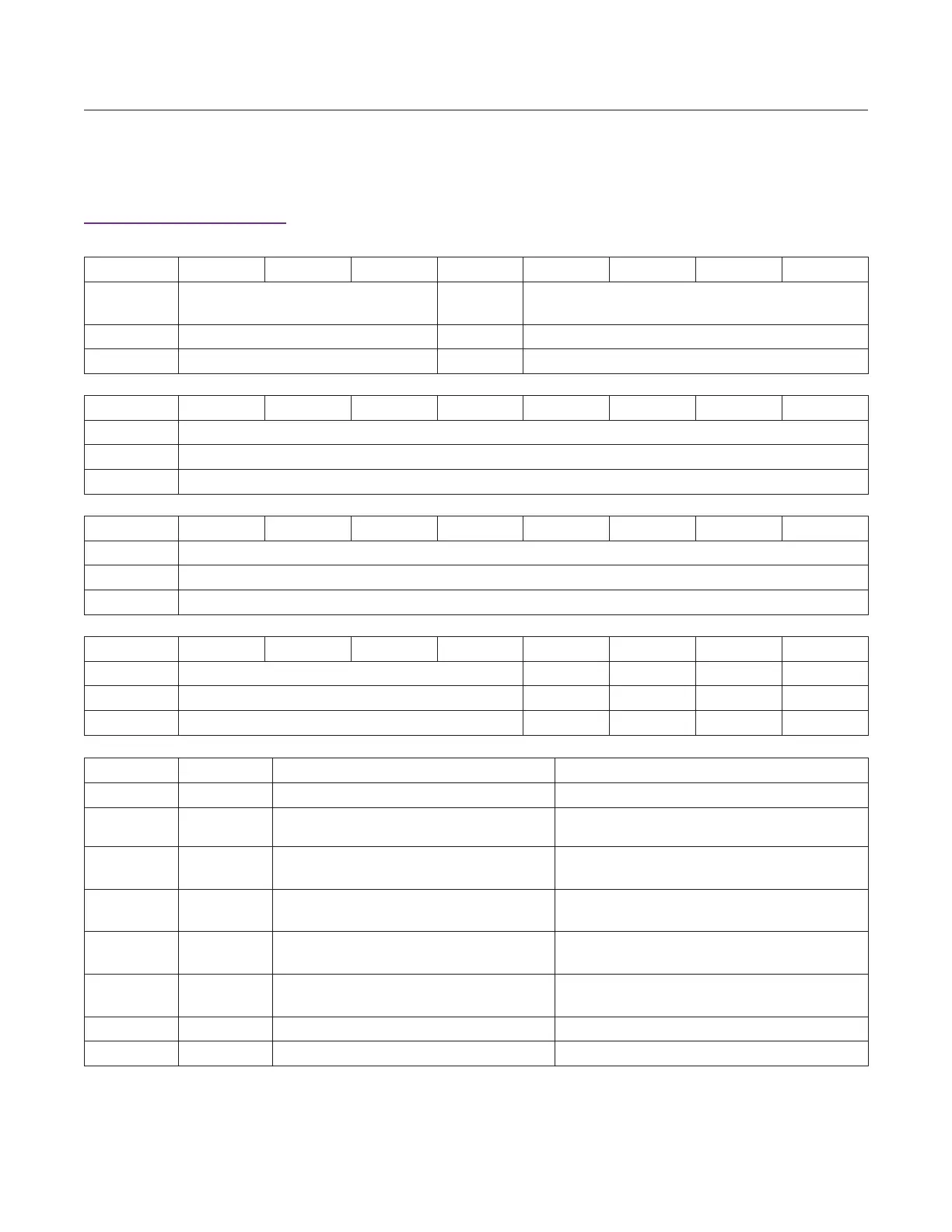
Clock Conguration 1 (0x7)
Clock Configuration
BIT 31 30 29 28 27 26 25 24
Field RESERVED[2:0]
EXTADC
CLK
REFCLK_L_CNT[11:8]
Reset 0x0 0x0 256
Access Type Write, Read Write, Read Write, Read
BIT 23 22 21 20 19 18 17 16
Field REFCLK_L_CNT[7:0]
Reset 256
Access Type Write, Read
BIT 15 14 13 12 11 10 9 8
Field REFCLK_M_CNT[11:4]
Reset 1563
Access Type Write, Read
BIT 7 6 5 4 3 2 1 0
Field REFCLK_M_CNT[3:0] FCLKIN ADCCLK RESERVED MODE
Reset 1563 0x0 0x0 0x1 0x0
Access Type Write, Read Write, Read Write, Read Write, Read Write, Read
BITFIELD BITS DESCRIPTION DECODE
RESERVED 31:29 Reserved: DO NOT CHANGE VALUE RESERVED
EXTADCCLK 28
Selects either internally generated or exter-
nally applied clock as ADC sampling clock
0x0: Use internally generated clock
0x1: Use clock provided on ADC_CLKIN pin
REFCLK_
L_CNT
27:16 Sets the value for the L counter
REFCLK_
M_CNT
15:4 Sets the value for the M counter
FCLKIN 3 Fractional clock divider selection
0x0: Bypass ADC clock divider
0x1: Take ADC clock from fractional divider
ADCCLK 2 ADC clock selection
0x0: Use output of reference clock divider/multiplier
0x1: Bypass reference clock divider/multiplier
RESERVED 1 Reserved: DO NOT CHANGE VALUE RESERVED
MODE 0 DSP interface mode selection
www.maximintegrated.com
Maxim Integrated
│
42
MAX2771 Multiband Universal GNSS Receiver