Table 6. Signal Assignments, GPIC to SKiiP 3 GD (Three-Phase Inverter)
Signal Inv. 0 (J26) Inv. 1 (J27)
Phase 1 Phase 2 Phase 3 Phase 1 Phase 2 Phase 3
High Side IGBT DO1 DO3 DO5 DO7 DO9 DO11
Low Side IGBT DO0 DO2 DO4 DO6 DO8 DO10
Current Sensor AI0± AI1± AI2± AI3± AI4± AI5±
DC Link Voltage AI7±
or AI_0
— — — — AI12±
or AI_5
Temperature Sensor — AI_1 — — AI_4 —
HALT DO_0,
DI_P0.0
DO_1,
DI_P0.1
DO_2,
DI_P0.2
DO_3,
DI_P0.3
DO_4,
DI_P0.4
DO_5,
DI_P0.5
GPIO DI_P0.7 — — — — DI_P0.12
Table 7. Signal Assignments, GPIC to Semikube GD (Three-Phase Inverter)
Signal Inv. 0 (J24) Inv. 1 (J25)
Phase 1 Phase 2 Phase 3 Phase 1 Phase 2 Phase 3
High Side IGBT DO1 DO3 DO5 DO7 DO9 DO11
Low Side IGBT DO0 DO2 DO4 DO6 DO8 DO10
Current Sensor AI0± AI1± AI2± AI3± AI4± AI5±
DC Link Voltage AI7±
or AI_0
— — — — AI12±
or AI_5
Temperature Sensor — AI_1 — — AI_4 —
HALT DO_0,
DI_P0.0
— — — — DO_5,
DI_P0.5
GPIO DI_P0.7 — — — — DI_P0.12
The signals on connectors 0 to 6 for SKiiP 3 GB and SKiiP 4, and signals on connectors 1 and
2 of SKiiP 3 GD and Semikube GB are shared. The two full bridge connectors for SKiiP 3 GD
and Semikube GD are also in parallel. One full bridge connector reuses signals from three
half-bridge connectors.
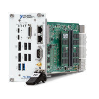
sbRIO-9687 User Manual | © National Instruments | 11
 Loading...