Safety
information
Product
information
Mechanical
installation
Electrical
installation
Getting
started
Running the
motor
Drive
parameters
Communications Diagnostics Technical data
UL Listing
Information
Commander S100 User Guide 99
8.1.3 MODBUS registers
The MODBUS register address range is 16 bit (65536 registers) which at
the protocol level is represented by indexes 0 through 65535.
PLC registers
Modicon PLCs typically define 4 register 'files' each containing 65536
registers. Traditionally, the registers are referenced 1 through 65536
rather than 0 through 65535. The register address is therefore
decremented on the master device before passing to the protocol.
The register file type code is NOT transmitted by MODBUS and all
register files can be considered to map onto a single register address
space. However, specific function codes are defined in MODBUS to
support access to the "coil" registers.
All standard CT drive parameters are mapped to register file '4' and the
coil function codes are not required.
Control Techniques parameter mapping
The MODBUS register address is 16 bits in size, of which the upper two
bits are used for data type selection leaving 14 bits to represent the
parameter address.
The table below shows how the start register address should be
calculated.
Data types
The MODBUS protocol specification defines registers as 16 bit signed
integers. All CT devices support this data size.
8.1.4 Data consistency
All CT devices support a minimum data consistency of one parameter
(16 bit or 32 bit data). Some devices support consistency for a complete
multiple register transaction.The Commander S100 only supports 16-bit.
8.1.5 Data encoding
MODBUS RTU uses a 'big-endian' representation for addresses and
data items (except the CRC, which is 'little-endian'). This means that
when a numerical quantity larger than a single byte is transmitted, the
MOST significant byte is sent first. So for example
16 - bits 0x1234 would be 0x12 0x34
8.1.6 Function codes
The function code determines the context and format of the message
data. Bit 7 of the function code is used in the slave response to indicate
an exception.
The following function codes are supported:
FC03 Read multiple
Read a contiguous array of registers. The slave imposes an upper limit
on the number of registers, which can be read. If this is exceeded the
slave will issue an exception code 2.
Table 8-1 Master request
Table 8-2 Slave response
FC06 Write single register
Writes a value to a single 16 bit register. The normal response is an echo
of the request, returned after the register contents have been written.
Table 8-3 Master request
Table 8-4 Slave response
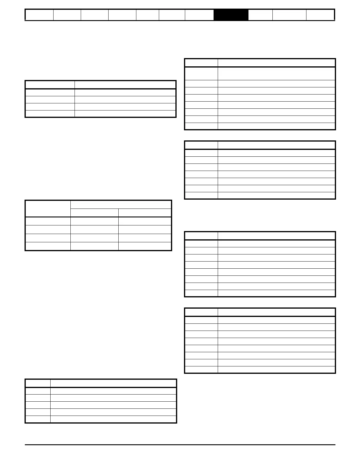
File type Description
1 Read only bits ("coil")
2 Read / write bits ("coil")
3 Read only 16bit register
4 Read / write 16bit register
Parameter
Protocol register
Decimal
Hex (0x)
m.pp m x 100 + pp -1
P1.04 103 00 67
P2.20 219 00 DB
P4.19 418 01 A2
Code Description
3 Read multiple 16 bit registers
6 Write single register
16 Write multiple 16 bit registers
23 Read and write multiple 16 bit registers
43 Read device identification (MEI type 14)
Byte Description
0
Slave destination node address 1 through 247, 0 is
global
1 Function code 0x03
2 Start register address MSB
3 Start register address LSB
4 Number of 16 bit registers MSB
5 Number of 16 bit registers LSB
6 CRC LSB
7 CRC MSB
Byte Description
0 Slave source node address
1 Function code 0x03
2 Length of register data in read block (in bytes)
3 Register data 0 MSB
4 Register data 0 LSB
3+byte count CRC LSB
4+byte count CRC MSB
Byte Description
0 Slave node address 1 through 247, 0 is global
1 Function code 0x06
2 Register address MSB
3 Register address LSB
4 Register data MSB
5 Register data LSB
6 CRC LSB
7 CRC MSB
Byte Description
0 Slave source node address
1 Function code 0x06
2 Register address MSB
3 Register address LSB
4 Register data MSB
5 Register data LSB
6 CRC LSB
7 CRC MSB