NVIDIA Jetson TX2/TX2i OEM Product Design Guide
JETSON TX2/TX2i OEM PRODUCT | DESIGN GUIDE | 20180618 99
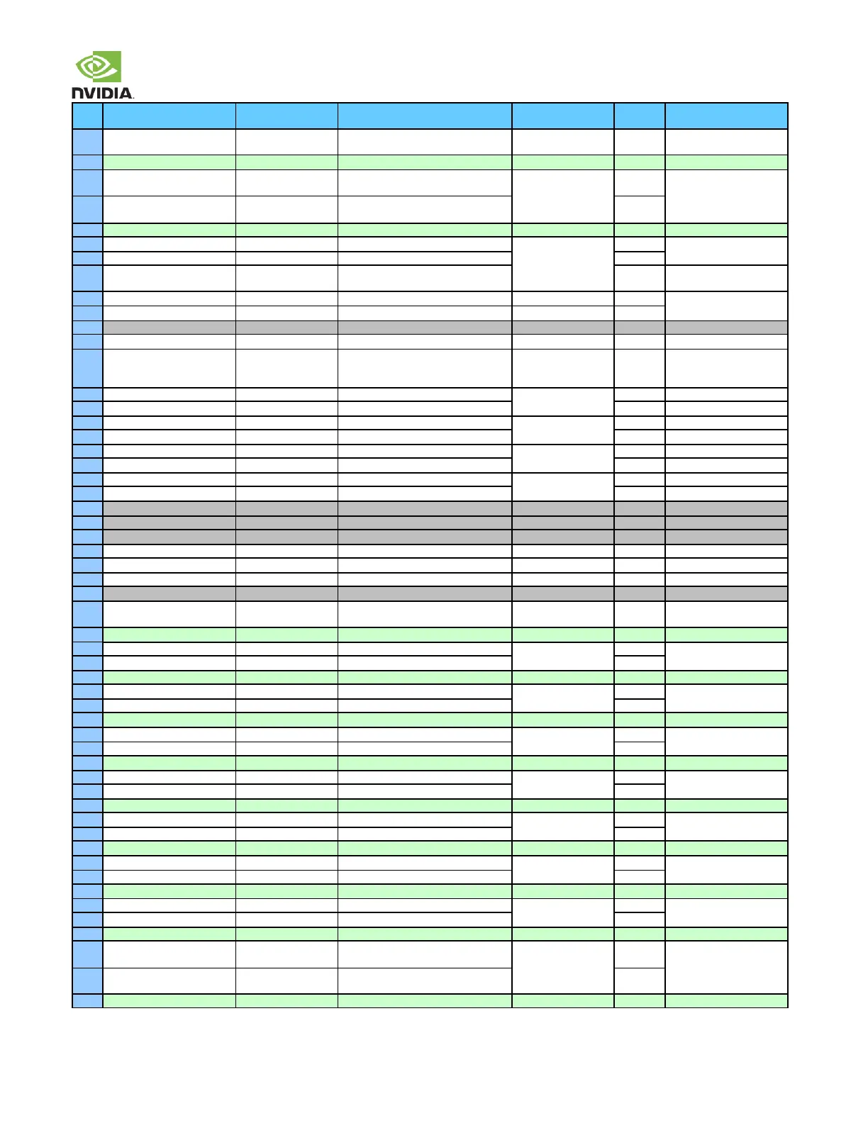
Usage on the Carrier
Board
PCIe RFU Transmit (PCIe IF #0 Lane 3
or USB 3.0 Port #1)
USB SS 1 Transmit+ (USB 3.0 Port #2 or
PCIe IF #0 Lane 1)
USB SS PHY, AC-Coupled on
carrier board
USB SS 1 Transmit (USB 3.0 Port #2 or
PCIe #0 Lane 1)
SATA PHY, AC-Coupled on
carrier board
SATA Device Sleep or PEX1_CLKREQ#
(PCIe IF #2) depending on Mux setting
Open Drain 3.3V, Pull-up on
the module
Open Drain 3.3V, Pull-up on
the module
PCIe 2 Reset (PCIe IF #1)
Sleep Request to the module from the
carrier board. An internal Tegra pull-up
is present on the signal.
SPI 0 Master In / Slave Out
DisplayPort 1 Lane 3 or HDMI Clk Lane
AC-Coupled on carrier
board
DisplayPort 1 Lane 3+ or HDMI Clk Lane+
DisplayPort 1 Lane 0 or HDMI Lane 2
AC-Coupled on carrier
board
DisplayPort 1 Lane 0+ or HDMI Lane 2+
PCIe 1 Transmit+ (PCIe #2 Lane 0 muxed
w/USB 3.0 Port #0)
USB 3.0 Type A
(Default) or M.2 Key E
PCIe PHY, AC-Coupled on
carrier board
PCIe 1 Transmit (PCIe #2 Lane 0 muxed
w/USB 3.0 Port #0)