Board Interface Connector
MPC5777C EVB User Guide, Rev. 1
29 NXP Semiconductors
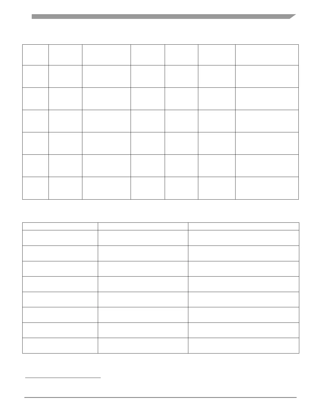
Table 18:
Jumper options for various power modes
J513
(1V25_SR_MB_SEL)
and J13 (SBC_1V25)
2
2&3 for LV
Linear
Regulator
J513- 3&4 for
1.25V_SR_OB1 (LR)
J13 - Open
J513- 5&6 for
1.25V_SR_OB2(SR)
J13 - Open
2&3 for LV
Linear
Regulator
J513- 3&4 for
1.25V_SR_OB1 (LR)
J13 - Open
J513- 5&6 for
1.25V_SR_OB2(SR)
J13 - Open
J513- 1&2 for
1.25V_SR_MB
-OR-
J13-1&2 for SBC_1V25
J513-1&2 for
1.25V_SR_MB
-OR-
J13-1&2 for SBC_1V25
Other Power supply Jumper settings:
Table 19:
MCU power selection jumpers
Jumper Setting (* - default)
1-2: 3.3V from onboard Power SBC
2-3: 3.3V from Mother Board*
1-2: 5V from onboard Power SBC
2-3: 5V from Mother Board*
IO Levels in the Mother Board -
VDD_HV_IO_MAIN
1-2: Select 3.3V
2-3: Select 5V*
ADC Analog Supply Selection
1-2: Select 5V from Linear Regulator*
2-3: Select 5V from Switching Regulator
Connect TRNG, Internal RC
oscillator Supply -VDDA_MISC
1-2: Connect VDDA_MISC to 5V_SR*
Connect SD ADC supply &
Reference –VDDA_SD, VRH_SD
J7, 1-2: Connect VDDA_SD*
J8, 1-2: Connect VRH_SD*
Connect eQADC supply &
Reference – VDDA_EQ, VRH_EQ
J9, 1-2: Connect VDDA_EQ*
J10, 1-2: Connect VRH_EQ*
Fast I/O Pads supply selection -
VDDE2
1-2: Select 3.3V*
2-3: Select 5V
CAUTION: For 1.25 V source selection, a single jumper must be installed on either J513 or J13, but not on both at a time.

 Loading...


