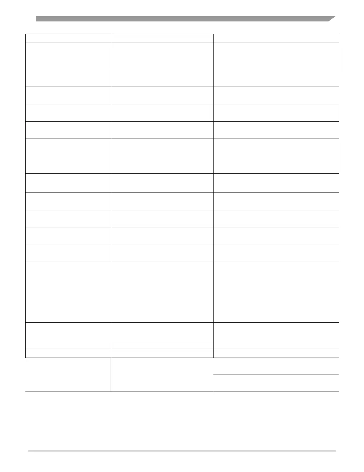
Board Interface Connector
MPC5777C EVB User Guide, Rev. 1
30 NXP Semiconductors
Jumper Setting (* - default)
RAM Standby supply selection -
VSTBY
1-3: Select 3.3 V
5-3: Select GND*
4-3: Select 5 V
SMPS Driver Supply Selection -
VDDPWR
1-2: Select 3.3 V
2-3: Select 5 V*
Core Supply generation, Regulation
Mode - REGSEL
1-2: Select SMPS Configuration (VDD_PMC)
2-3: Select Linear Configuration (GND)*
PMC Supply Selection – VDDPMC
1-2: Select 3.3 V
2-3: Select 5 V*
Core Supply generation, Regulator
Control -REGCTL
1-2: Select SMPS to derive (1.25V_SR_OB2)
2-3: Select Linear to derive (1.25V_SR_OB1)*
VDD Core Supply Selection
1-2: 1.25 V from Mother Board*
3-4: 1.25 V onboard Regulator (Linear Mode)
5-6: 1.25 V onboard Regulator (Switching
Mode)
VDD Core Supply Selection
1-2: 1.25 V from onboard Power SBC
Medium I/O Pads supply selection –
VDDEH3A
1-2: Select 3.3 V
2-3: Select 5 V*
Connect Flash Core Supply -
VDDFLA
1-2: Connect VDDFLA to 3.3V_SR
Fast I/O Pads supply selection -
VDDE2A
1-2: Select 3.3 V*
2-3: Select 5 V
Medium I/O Pads supply selection -
VDDEHx
1-2: Select 3.3 V
2-3: Select 5 V*
Medium I/O Pads supply enable –
VDDEHx
1-2: Connect VDDEH1*
3-4: Connect VDDEH3*
5-6: Connect VDDEH4*
7-8: Connect VDDEH5*
9-10: Connect VDDEH6*
11-12: Connect VDDEH7*
All jumpers in J30 placed by Default
JTAG IO Level - VDD_HV_IO_JTAG
1-2: Select 3.3 V*
2-3: Select 5 V
1-2: Connect LED with Signal ETPUA0*
1-2: Connect LED with Signal ETPUA1*

 Loading...


