Specifications Operation Manual
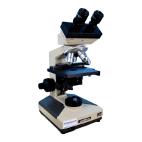
Microscopic observation
range
φ300 mm
Stage height stroke
Up and down from observation position by 1 mm
Standard inspection
magnification
Up to 50X objective
Wafer table
Conductive PEEK resin
Wafer holding method
Vacuum adsorption (Vacuum supplied by the loader)
Stage Weight
Approx. 12 kg
Anti-Vibration table
Spring-type vibration isolator
5. Inspection Mode
All (100%) inspection
Continuous transfer (Two wafers at a time are transferred)
Sampling transfer patterns
10 patterns (P1 to P10) can be registered.
Transfer of specified wafers (Two wafers at a time are transferred) (When one wafer is
being inspected under the microscope, the next wafer is being transferred to the macro
Sampling inspection
patterns
10 patterns (L1 to L10) can be registered.
Transfer and inspection of specified wafers (One wafer is transferred at a time)
Automatic skip function
Slots with no wafer are automatically skipped in both the All and Sampling modes.
6. Auxiliary Functions during Inspection
Wafer registration
Numbers of defective wafers registered in each type of inspection can be displayed
Pause
When the inspection time is set to 0 - 8 seconds, it can be extended by pausing
the loader.
Wafer removal
Wafers can be removed by using tweezers or similar tools during inspection.
Wafer alignment(Notched)
Contactless detection using the opto-sensor
Four notched positions (the near, far, right and left sides) can be selected on the
microscope stage at 90-degree intervals.
Settings can be changed during inspection. (The position specified before the notched
Wafer alignment
Contactless alignment (optical)
7. Protective Functions
Emergency stop
EMO switch (primary power shut down turns off the main power of the system. When
EMO switch is released , the main power stays turned off)
Wafer popping
Wafers popping out of a cassette can be detected.
Warnings and error display
The liquid crystal panel shows error codes and their details.
An error log can be displayed and obtained.
Wafers in the cassette
Any slanted wafers can be detected (1st-slot cross).
Stage lock
The stage position can be locked until the wafer is transferred onto the microscope
completely
Wafer protection in case of
power failure
Wafers are held in case of power failure.
8. Transfer Mechanism
Wafer transfer method
Wafer back side vacuum adsorption and mechanical arm transfer
Wafer contact area material
Back side of wafer : PEEK (polyetheretherketone) resin
Edge of wafer : polyacetal resin
(
)
Wafer contact area
Back side of wafer, Edge of wafer (when inspecting the back side)
Noise level during transfer
69 dB(A) or lower
 Loading...