RZ/A2M SUB Board RTK79210XXB00000BE 2. Function specifications
R20UT4398EJ0100 Rev.1.00 2-26
2018.10.11
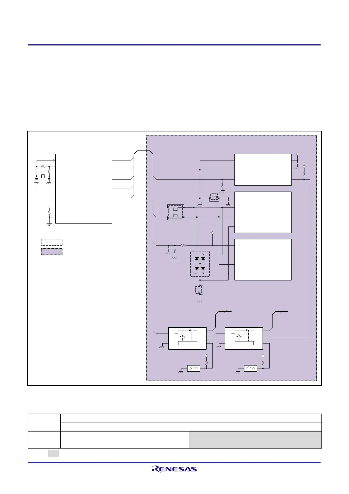
2.4 USB Interface
RTK79210XXB00000BE is equipped with a USB series A port x 1 and USB Mini-B port x 1 as the standard
configuration of USB connectors.
However, USB interface pins are shared by the Series A port pins and Mini-B port pins, therefore Series A port and
Mini-B port cannot be used at the same time.
Figure 2.4.1 shows USB interface block diagram, and Table 2.4.1 shows the functions setting tables of DIP switches
SW6-1 and SW6-3 for system setting.
Figure 2.4.1 USB Interface Block Diagram
Table 2.4.1 Function Setting Table of DIP Switches SW6-1 and SW6-3 for System Setting
RZ/A2M (U1)
DP1
5
P7_5 / CKE / DRP08 / CTS1 /
OVRCUR1
DM1
DP1
DM1
PC_5 / VBUSEN1
DM1
DP1
48MHz
(X2)
USB_X1
USB_X2
RREF
USBAVss
PC_0 / VBUSIN1
VBUS1
EN1
EN1
USB Type-A receptacle(CN12)
D-
VBUS
D+
VBUS power source control
IC (U29)
EN
INOUT1
FLG
5V
USB Mini-B receptacle(CN13)
D-
VBUS
D+
VBUS1
SDRAM /
Other(USB)(U12)
1
To SDRAM
3.3V
DIP
SW6-1
DRP /
Other(USB)(U11)
1
3.3V
DIP
SW6-3
MUXOE# S
3A
3B1
3B2
MUXOE# S
4A
4B1
4B2
To DRP I/F
FLG
OFF OFF
1 2
4 3
VBUS
3.3V
OC1#
OC1#
FG[1:2]
FRAME
OC1#
OUT2
Note: Red text indicates a function used.
:Indicates a function not implemented.
: Indicates a SUB board.
2.2k±1%
+
150F
1k
1F
1F
ON(L):A=B1, OFF(H):A=B2 ON(L):A=B1, OFF(H):A=B2
1.8k
 Loading...


