RZ/A2M SUB Board RTK79210XXB00000BE 2. Function specifications
R20UT4398EJ0100 Rev.1.00 2-42
2018.10.11
2.17 DRP Interface
RTK79210XXB00000BE is equipped with a 40 pin MIL connector, which allows interface with the RZ/A2M DRP
interface.
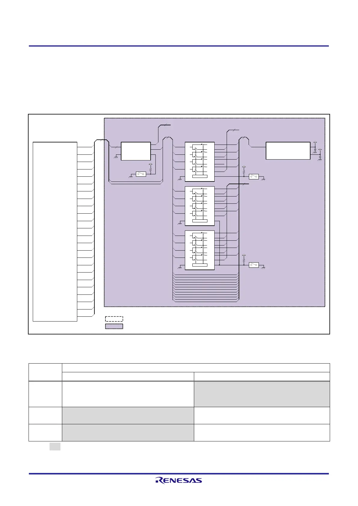
Figure 2.17.1 shows the DRP interface block diagram, and Table 2.17.1 shows the function setting table of DIP
switches SW6-1, SW6-2, and SW6-3 for system setting.
Figure 2.17.1 DRP Interface Block Diagram
Table 2.17.1 Function Setting Table of DIP Switches SW6-1, SW6-2, and SW6-3 for System Setting
P1_0 and P0_[6 :0], P8_[7 :1], P9_[7 :0], P7_[5 :3],
P7_[1 :0], P6_7, P6_5 are used as SDRAM control
pins.
P1_0 and P0_[6 :0], P8_[7 :1], P9_[7 :0], P7_[5 :3],
P7_[1 :0], P6_7, P6_5 are used as DRP pins (default
setting).
P8_4 and P8_[7 :6], P6_4, P9_[6 :3] are used as
DRP pins.
P8_4 and P8_[7 :6], P6_4, P9_[6 :3] are used as
audio interface pins (default settings).
P9_[1 :0] and P1_0, P7_5 are used as DRP pins.
P9_[1 :0] and P7_5 are used as UART or USB
interface pins (default settings).
[Note] indicates setting functions.
32
P1_0
DRP [30:24]
DRP [23:21]
P8_4
DRP19
P8_6
P8_7
P9_0
P9_1
DRP[31:0]
DRP connector(CN2)
DRP[31:0]
3.3V
5V
SDRAM / Other(DRP)
DRP02
OE# S
A
B2
P6_4
DRP14
P9_3
32
30
DRP[30:24]
DRP[23:21]
8
To Audio I/F
32
P9_4
P9_5
P9_6
DRP09
P7_5
DRP07
DRP06
DRP05
DRP04
DRP03
DRP02
DRP01
P6_4
P1_0 / D7 / DRP31
P0_[6:0] / D[6:0] / DRP[30:24]
P8_[1:3] / A[1:3] / DRP[23:21]
P8_4 / A4 / DRP20 / SSL00
P8_5 / A5 / DRP19 / MISO0
P8_6 / A6 / DRP18 / MOSI0
P8_7 / A7 / DRP17 / RSPCK0
P9_0 / A8 / DRP16 / TxD4
P9_1 / A9 / DRP15/ RxD4
P9_2 / A10 / DRP14
P9_3 / A11 / DRP13 / SSIRxD0
P9_4 / A12 / DRP12 / SSITxD0
P9_5 / A13 / DRP11 / SSIFS0
P9_6 / A14 / DRP10 / SSIBCK0
P9_7 / A15 / DRP09
P7_5 / CKE / DRP 08 / CTS1 /
OVRCUR1
P7_4 / CAS / DRP07 / RTS1
P7_3 / RAS / DRP06 / TxD1
P7_1 / RD/WR / DRP05 / RxD1
P7_0 / WE1/DQMU / DRP04 /
SCK1
P6_7 / WE0/DQML / DRP03
P6_6 / DRP 02
P6_5 / CS3 / DRP01
P6_4 / DRP 00/ AUDIO_CLK
RZ/A2M (U1)
3.3V
DIP
SW6-1
DRP14
DRP09
DRP07
DRP06
OFF
DRP05
DRP04
DRP03
DRP02
DRP01
DRP / Audio(U6)
DRP13
DRP12
DRP11
DRP10
P9_3
P9_4
P9_5
P9_6
MUXOE# S
4A
4B1
4B2
3A
3B1
3B2
2A
2B1
2B2
1A
1B1
1B2
DRP / Audio(U3)
DRP20
DRP18
DRP17
DRP00
P8_4
P8_6
P8_7
P6_4
MUXOE# S
4A
4B1
4B2
3A
3B1
3B2
2A
2B1
2B2
1A
1B1
1B2
DRP / Other(U11)
DRP16
DRP15
DRP31
DRP08
P9_0
P9_1
P1_0
P7_5
MUXOE# S
4A
4B1
4B2
3A
3B1
3B2
2A
2B1
2B2
1A
1B1
1B2
DIP
SW6-3
3.3V
ON
To UART I/F, USB(ch1)
DIP
SW6-2
3.3V
ON
3
MUX×8
DRP19
Note: Red text indicates a function used .
:Indicates a function not implemented .
:Indicates a SUB board.
ON(L):A=B1, OFF(H):A=B2
ON(L):A=B1, OFF(H):A=B2
B1
30
To SDRAM
 Loading...


