RZ/A2M SUB Board RTK79210XXB00000BE 2. Function specifications
R20UT4398EJ0100 Rev.1.00 2-34
2018.10.11
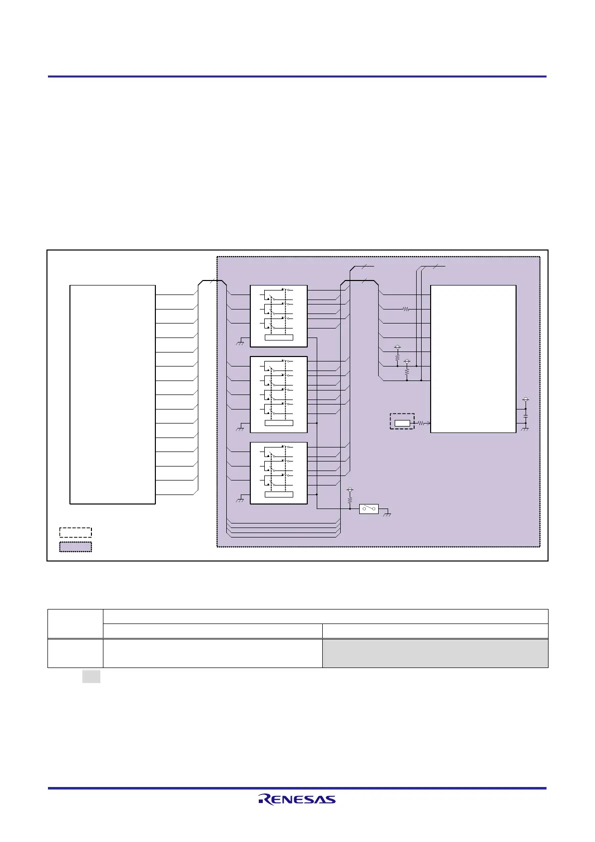
2.11 CMOS Camera Interface
RZ/A2M is equipped with an on-chip capture engine unit (CEU) that captures digital image data externally input, and
transfers the data to memory. On RTK79210XXB00000BE, CEU pins of RZ/A2M connect with 26 pin MIL pitch
connector to enable connection with various CMOS cameras.
X6 can be connected to an oscillator to input a sampling clock externally for the CMOS camera.
A pull-up resistor for I2C-bus is already mounted on RTK79210XXB00000BE, therefore it is not needed for the
CMOS camera side.
Figure 2.11.1 shows CMOS camera interface block diagram, and Table 2.11.1 shows a function setting table of DIP
switch SW6-4 for system setting.
Figure 2.11.1 CMOS Camera Interface Block Diagram
Table 2.11.1 Function Setting Table of DIP Switch SW6-4 for System Setting
PE_1
22
P6_1
PE_0
PE_6
P6_3
PE_3
PE_4
PE_2
PE_5
P6_2
D[11:8]
D[1:0]
D[15:12]
Ether1 / CEU(U13)
D[15:8]
D[1:0]
Ether1 / CEU(U16)
Ether1 / CEU(U18)
22
10
To EthernetPHY1
P6_3
P6_2
P6_1
PE_3
PE_1
PE_2
PE_0
PE_4
PE_5
CMOS camera connector (CN17)
D[15:0]
CLK
D[15:0]
CLK
HD
FLD
VD
SDA3
HD
VD
FLD
SDA
SCL3
SCL
REFCLK
HD
VD
CLK
D6
D7
D5
FLD
D3
D4
DIP
SW6-4
3.3V
MUXOE# S
3A
3B1
3B2
2A
2B1
2B2
1A
1B1
1B2
MUXOE# S
3A
3B1
3B2
2A
2B1
2B2
1A
1B1
1B2
MUXOE# S
4A
4B1
4B2
3A
3B1
3B2
2A
2B1
2B2
1A
1B1
1B2
SCL3
SDA3
RZ/A2M (U1)
PE_1 / ET0_RXD0/RMII0_RXD0 /
VIO_D7
PE_2 / ET0_RXD1/RMII0_RXD1 /
VIO_D6
PE_3 / ET0_RXER/RMII0_RXER /
VIO_D5
PE_4 / ET0_CRS/RMII0_CRSDV /
VIO_D4
PE_5 / ET0_MDC / VIO_D3
PE_6 / ET0_MDIO / VIO_D2
PE_0 / ET0_RXCLK/REF50CK0 /
VIO_FLD
P6_3 / ET0_TXD1/RMII0_TXD1 /
VIO_HD
P6_2 / ET0_TXD0/RMII0_TXD0 /
VIO_VD
P6_1 / ET0_TXEN/RMII0_TXDEN /
VIO_CLK
PG_[4:7] / VIO_D[15:12]
PG_[3:0] / VIO_D[11:8]
PH_[0:1] / VIO_D[1:0]
PD_6 / RIIC3SCL
PD_7 / RIIC3SDA
3.3V
SCL3
SDA3
CLK
Socket(X6)
3.3V
VCC
GND
OFF
2
To EEPROM, LCD I/F
PE_6
D2
3.3V
Note: Red text indicates a function used .
:Indicates a function not implemented .
:Indicates a SUB board .
ON(L):A=B1, OFF(H):A=B2
 Loading...


