R301 RF POWER SUPPLY OPERATOR’S MANUAL
TYPICAL INTERFACE CIRCUITS
Figures 1 through 5 illustrate the typical circuits used in the R301 RF Power Supply’s
Analog Interface.
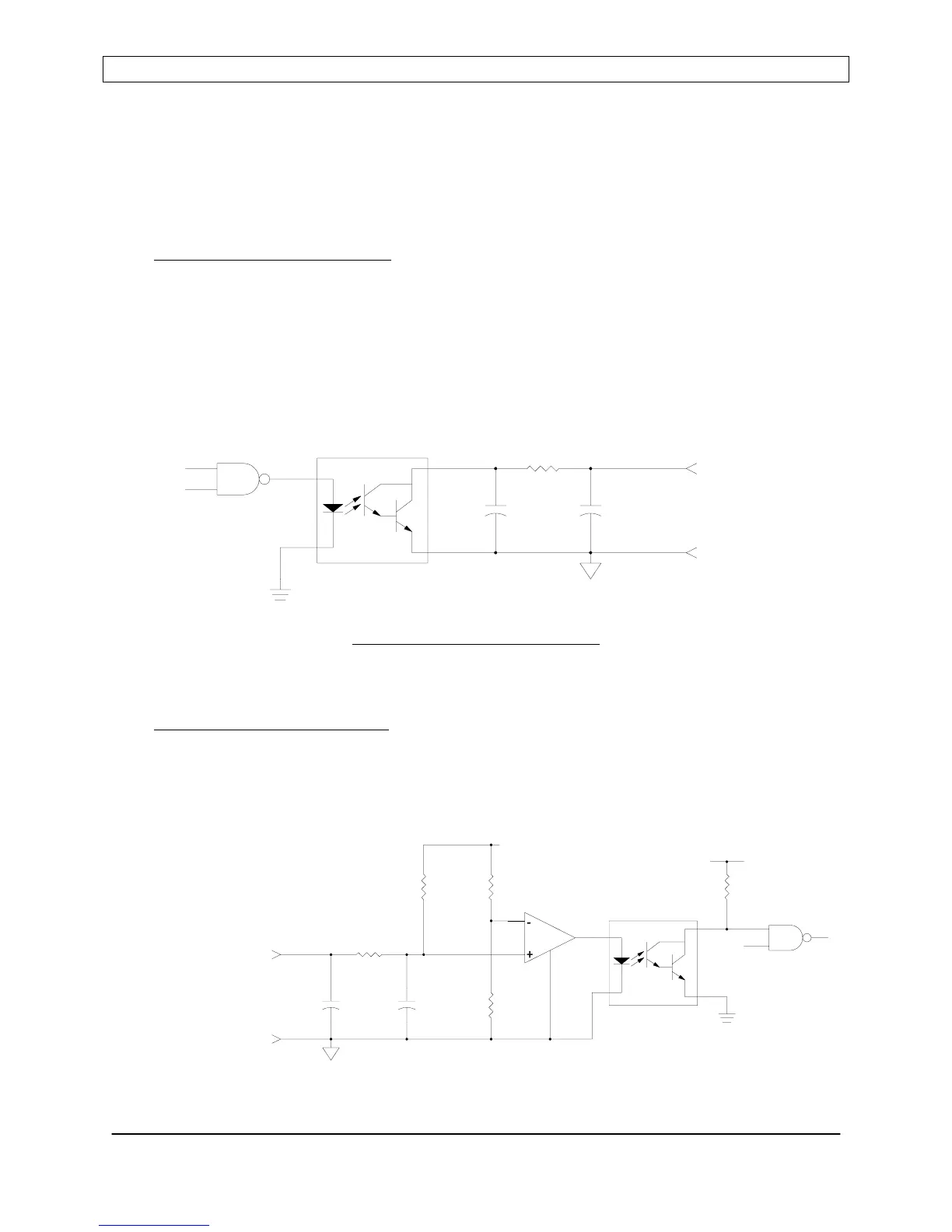
RFENABLED* Output Circuit:
RF output status signal. Active low, open collector output. 12VDC maximum, 15mA
maximum current sink, 150mW maximum power dissipation.
Signal output is closed (0V or “low”) for an RF on condition; signal output is “open” for an
RF off condition.
Figure 1: RFENABLED* Circuit
TTL-Compatible Input Circuits
All TTL-Compatible logic input circuits are internally pulled up to +5VDC. Signal
function and response is as described in the Analog Interface Connector pin list.
Page 41
Seren IPS Inc.
6100130000 Rev. 0.05
100
0.1uF
0.1uF
(GNDI)
RETURN
RFENABLED*
100K
0.1uF
100
0.1uF
10K
LM339
10K
+5I
TTL INPUT
RETURN
(GNDI)
+5V
 Loading...