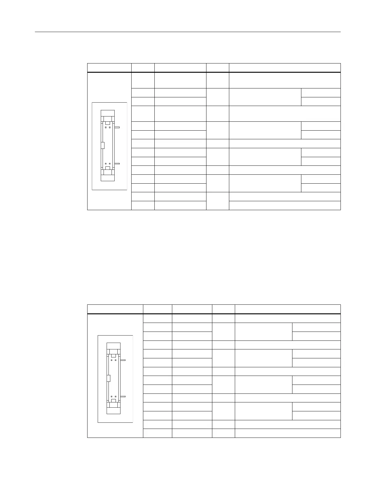
DVI-I interface
Table 1-11 Assignment of DVI-I interface
Connector Pin Name Type Remark
S GND - Ground
S1 GND - Ground
C1 R
O
Red
C2 G Green
C3 B Blue
C4 HSYNC O Horizontal synchronizing pulse
C5 GND - Ground
CSA GND - Ground
1 TX2N
O
TDMS data 2-
2 TX2P TDMS data 2+
3 GND - Ground
4 N.C. - Not connected
5 N.C. - Not connected
6 DDC CLK
B
DDC clock
7 DDC CLK DDC data
8 VSYNC O Vertical synchronizing pulse
9 TX1N
O
TDMS data 1-
10 TX1P TDMS data 1+
11 GND - Ground
12 N.C. - Not connected
13 N.C. - Not connected
14 + 5 V VO + 5 V
15 GND VO Ground
16 MONDET I Hot plug detect
17 TX0N
O
TDMS data 0-
18 TXoP TDMS data 0+
19 GND - Ground
20 N.C. - Not connected
21 N.C. - Not connected
22 GND - Ground
23 TXCP
O
TDMS clock +
24 TXCN TDMS clock -
I/O USB interface
All signals required for connecting operator panel fronts, with the exception of the display
interface, are assigned to this interface.
Associated interface cable: K1
Connector type: 2 x 13-pin socket connector
General information and networking
1.3 Connecting
Handheld Terminal HT 8
Manual, 07/2015, A5E36371621B-AB 29
 Loading...