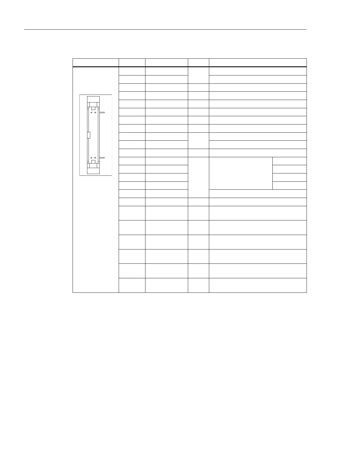
Table 1-9 Assignment of the Ethernet RJ45 interface 10/100 Mbit/s
Connector Pin Name Type Remark
1 TxD+
O Transmit data
2 TxD-
3 RxD+ I Receive data
4/5 GND - (terminated internally with 75 Ω; not re‐
quired for data transmission)
6 RD- I Receive data
7/8 GND - (terminated internally with 75 Ω; not re‐
quired for data transmission)
Shield - - On connector housing
- Green LED
(right)
- Lights up: 10 or 100 Mbit/s
Off: No or faulty connection
- Orange LED
(left)
- Illuminated: Data exchange
Off: No data exchange
Table 1-10 Assignment of the Ethernet RJ45 interface 1000 Mbit/s
Connector Pin Name Type Remark
1 DA+ B Bidirectional pair A+
2 DA- Bidirectional pair A-
3 DB+ Bidirectional pair B+
4 DC+ Bidirectional pair C+
5 DC- Bidirectional pair C-
6 DB- Bidirectional pair B-
7 DD+ Bidirectional pair D+
8 DD- Bidirectional pair D-
Shield - - On connector housing
- Green LED
(right)
- Illuminated orange: 1000 Mbit/s
Off: No or faulty connection
- Orange LED
(left)
- Illuminated: Data exchange
Off: No data exchange
Note
Connection only on LAN, not on telecommunication networks!
General information and networking
1.3 Connecting
Handheld Terminal HT 8
28 Manual, 07/2015, A5E36371621B-AB
 Loading...