SPC3 PROFIBUS Interface Center
SPC3 Hardware Description V1.3 Page 9
Copyright (C) Siemens AG 2003 All rights reserved. 2003/04
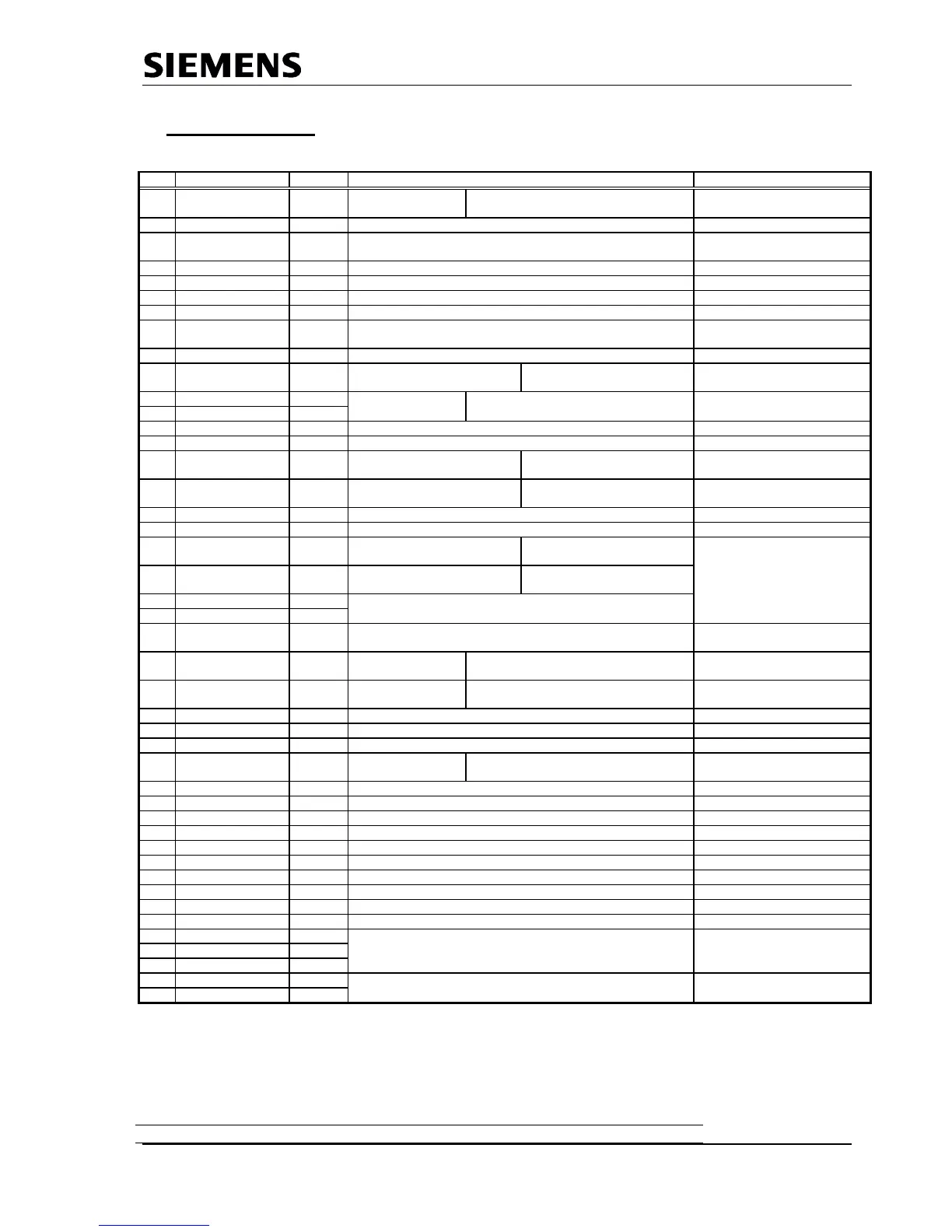
3 Pin Description
The SPC3 has a 44-pin PQFP housing with the following signals:
Pin
Signal Name In/Out Description Source / Destination
1 XCS I© Chip-Select C32 Mode: place on VDD.
C165 Mode: CS-Signal
CPU (80C165)
2 XWR/E_Clock I© Write signal /EI_Clock for Motorola CPU
3 DIVIDER I© Setting the scaler factor for CLK2OUT2/4.
low potential means divided through 4
4 XRD/R_W I© Read signal / Read_Write for Motorola CPU
5 CLK I(TS) Clock pulse input System
6 VSS
7 CLKOUT2/4 O Clock pulse divided by 2 or 4 System, CPU
8 XINT/MOT I© <log> 0 = Intel interface
<log> 1 = Motorola interface
System
9 X/INT O Interrupt CPU, Interrupt-Contr.
10 AB10 I(CPD) Address bus C32 mode: <log> 0
C165 mode: address bus
11
DB0 I©/O Data bus C32 Mode: Data/address bus multiplexed CPU, memory
12
DB1 I©/O C165 Mode: Data/address bus separated
13
XDATAEXCH O Data_Exchange state for PROFIBUS-DP LED
14
XREADY/XDTACK O Ready for external CPU System, CPU
15
DB2 I©/O Data bus C32 mode: data bus/address
bus multiplexed
CPU, memory
16 DB3 I©/O C165 mode: data/address bus
separate
17
DB4
I©/O
Data bus C32 mode: data bus/address
bus multiplexed
20
DB5 I©/O C165 mode: data bus/address
bus separate
CPU, memory
21
MODE I <log> 0 = 80C166 Data bus/address bus separated; ready signal
<log> 1 = 80C32 data bus/address bus multiplexed, fixed timing
System
24
ALE/AS I© Address latch enable C32 mode: ALE
C165 mode: <log> 0
CPU (80C32)
25
AB9 I Address bus C32 mode: <log> 0
C165 mode: address bus
CPU (C165), memory
26
TXD O Serial send port RS 485 sender
27
RTS O Request to Send RS 485 sender
28
AB8 I© Address bus C32 Mode : <log> 0
C165 Mode: address bus
30
RXD I© Serial receive port RS 485 receiver
31
AB7 I© Address bus System, CPU
32
AB6 I© Address bus System, CPU
33
XCTS I© Clear to send <log> 0 = send enable FSK modem
34
XTEST0 I© Pin must be placed fixed at VDD.
35
XTEST1 I© Pin must be placed fixed at VDD.
36
RESET I(CS) Connect reset input with CPU’s port pin.
37
AB4 I© Address bus System, CPU
38
AB2 I© Address bus System, CPU
42
AB1 I© Address bus System, CPU
44
AB0 I©
Figure 3.1: SPC3 Pin Assignment
Note: •
••
• All signals that begin with X.. are LOW active
• VDD = +5V, VSS = GND
Input levels: I ©: CMOS
I (CS): CMOS Schmitt trigger