SPC3 PROFIBUS Interface Center
SPC3 Hardware Description V1.3 Page 49
Copyright (C) Siemens AG 2003 All rights reserved. 2003/04
8.5.3 Timing in the Asynchronous Intel Mode (X86 Mode) :
In 80X86 operation, SPC3 acts like memory with ready logic. The access times depend on the type of
accesses.
The request for an access to SPC3 is generated from the negative edge of the read signal or the positive
edge of the write signal.
SPC3 generates the Ready signal synchronously to the fed in pulse. The Ready signal is reset when the
read signal or write signal is deactivated. The data bus is switched to the Tristate with XRD = 1.
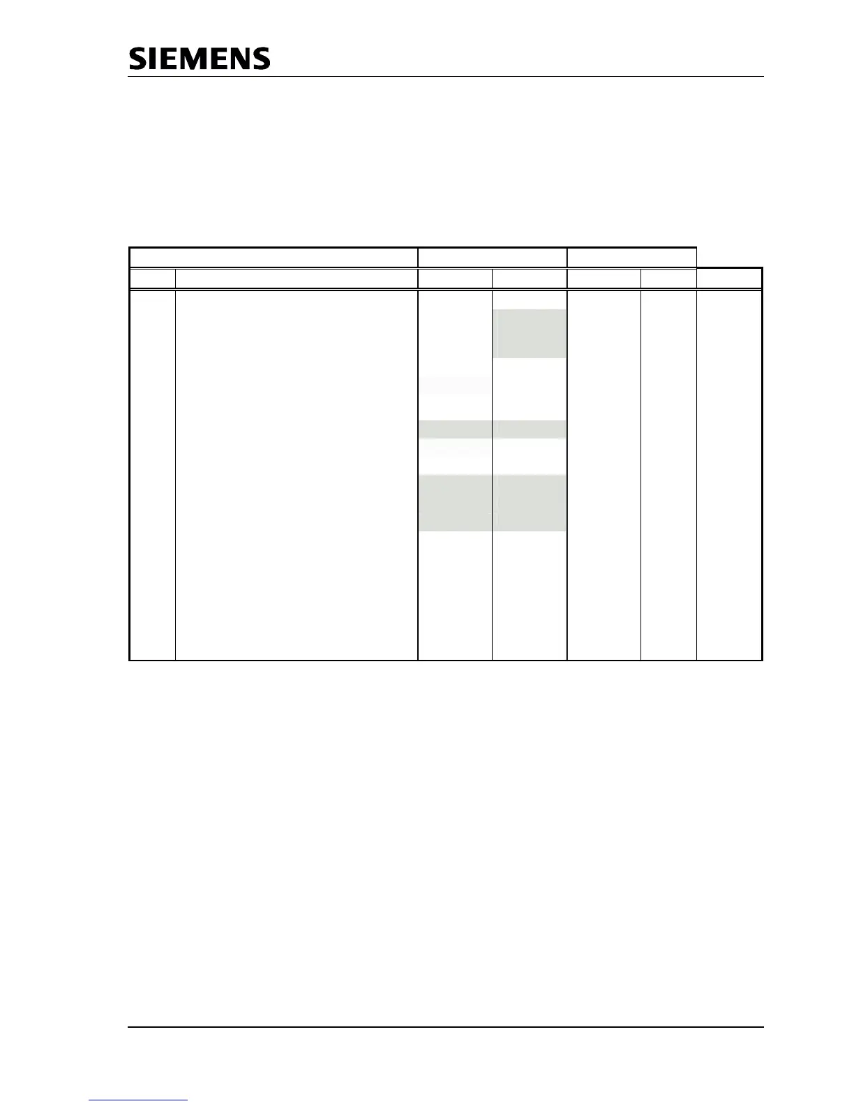
AMI-Vers.
ST-Vers.
No. Parameter Min Max Min Max Unit
20
Address-Setuptime to RXD ↓ or XWR ↓
0
0
ns
21
XRD ↓ to Data valid (Zugriff auf RAM)
4T+5
(88,3)
3T+42.5
(105)
ns
XRD ↓ to Data valid (Zugriff auf die Register)
4T+18
(101,3)
4T+20.2
(103,5)
ns
22
Address (AB
10..0
) Holdtime after XRD or XWR ↑
0
0
ns
23
XCS ↓ Setuptime to XRD ↓ or XWR ↓
- 5
-5
ns
24 XRD-Puls-Width 6T – 10
(115)
6T
−
10
(115)
ns
25
Data Holdtime after XRD ↑
2 6
3.1 10.2
ns
26 Read/Write-Inactive-Time 10
10
ns
27
XCS Holdtime after XRD ↑ or XWR ↑
0
0
ns
28
XRD/XWR ↓ to XRDY ↓ (Normal Ready)
4T + 5 5T+ 14
5T + 16
ns
29
XRD/XWR ↓ to XRDY ↓ (Early Ready)
3T + 5 4T+ 14
4T + 12
ns
30 XREADY-Holdtime after XRD or XWR 4.3 12.8
6 22
ns
31
Data Setuptime to XWR ↑
10
10
ns
32
Data Holdtime after XWR ↑
10
10
ns
33 XWR-Pulse-Width * 4T
4T
ns
34 XRD, XWR Cycletime 6T
6T
ns
35
last XRD
to XCS
4T + 10
4T + 10
ns
36
XCS
to next XWR
2T + 10
2T + 10
ns
37
XWR
to next XWR (XCS don’t care)
6T
6T
ns
Explanations:
T = Clock pulse cycle (48MHz)
TBD = to be defined
(1
= Access to the RAM
(2
= Access to the registers/latches
(3
= For T = 48 MHz