NANYTE BEAM Manual
NANYTE BEAM Manual BM-001-A3 / V1.1a Page 20 of 33
Patterning
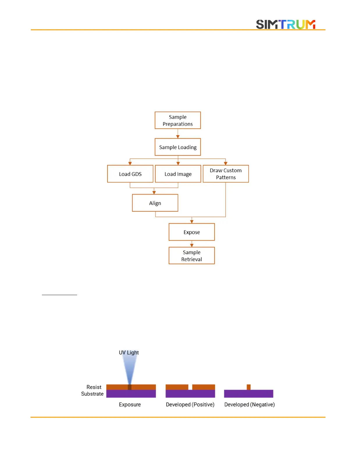
NANYTE BEAM was designed so that the least number of steps are necessary to do a full
exposure. Depending on the complexity of the patterning job, it is possible to load, align and
expose a pattern onto a wafer in under 3 minutes. The flow of the entire patterning process is
as shown below:
Sample preparation and loading
Spin coating
The first step in photolithography is to spin coat a layer of photoresist on to the sample surface.
The BEAM ENGINE uses h-line or 405 nm UV radiation for exposure; thus, an appropriate
photoresist has to be used. Other than spectral sensitivity, it is important to verify that the resist
is of the correct type (positive/negative, see below), and that the thickness is suitable for the
required resolution/aspect ratio.
www.simtrum.com