SOFAR 3.3K~12KTL-X User manual
All rights reserved
© Shenzhen SOFARSOLAR Co ., Ltd.
Figures and Tables
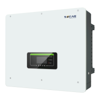
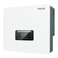
Figure 2-1Interface figure .......................................................................... 12
Figure 2-2 Inverter front & side dimensions .............................................. 13
Figure 2-3 Overview of the grid configurations ......................................... 14
Figure 3-1 Installation flowchart ................................................................ 17
Figure 3-2 Wall clearances for single inverter ........................................... 22
Figure 3-3 Wall clearances for multiple inverters ...................................... 22
Figure 3-4 Wall mount procedure .............................................................. 23
Figure 4-1 Cable connection flowchart ...................................................... 24
Figure 4-2 Grounding connection instruction (1) ....................................... 24
Figure 4-3 Grounding connection instruction (2) ....................................... 25
Figure 4-4 Inverter ground terminal placement .......................................... 26
Figure 4-5AC output cable assembly ......................................................... 28
Figure 4-6 Cable connection schematic diagram........................................ 28
Figure 4-7 WIFI/RS485 location ................................................................ 29
Figure 4-8 Waterproof RJ45 connector assembly ...................................... 29
Figure 4-9 RS485 wiring pinout(1) ............................................................ 30
Figure 4-10 RS485 Connecting communications cable(2) ......................... 30
Figure 4-11 RS485 Connecting communications cable(3) ......................... 30
Figure 4-12 Single inverter communications ............................................. 31
Figure 4-13 Multiple inverter communications .......................................... 32
Figure 4-14 Connect multiple Wifi to wireless router ................................ 33
Figure 4-15 DRM port ................................................................................ 33
Figure 4-16 Positive MC4 connector ......................................................... 35
Figure 4-17 Negative MC4 connector ........................................................ 36
Figure 4-18 Stripping length of DC cable .................................................. 37
Figure 4-19 Assemble the crimped MC4 ................................................... 37
Figure 4-20 Connecting DC input power cable .......................................... 38
Figure 4-21 Removing a DC input connector ............................................ 38
Figure 4-22 DRMs port location ................................................................ 39
Figure 4-23 DRMs wiring scheme ............................................................. 40
 Loading...