97
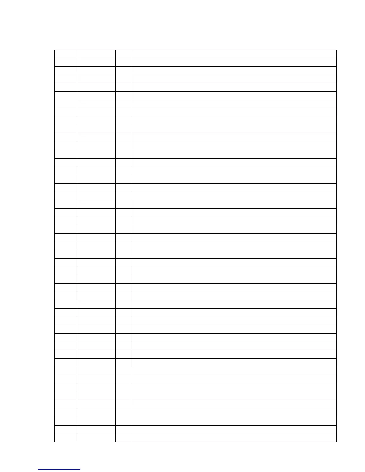
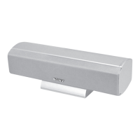
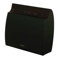
HCD-C770/C990
Pin No. Pin Name I/O Description
116 RFDCC I
Input terminal for adjusting DC cut high-pass filter for RF signal Not used
117 RFIN I
RF signal input from the DVD/CD RF amplifier
118, 119 VCCA5, VCCA4 —
Power supply terminal (+3.3V) (analog system)
120 VCOR1 —
VCO oscillating range setting resistor connected terminal
121 VCOIN I
VCO input terminal
122, 123 GNDA4, GNDA3 —
Ground terminal (analog system)
124 LPF5 O
Signal output from the operation amplifier from PLL loop filter
125 VC1 I
Middle point voltage (+1.65V) input terminal
126, 127 LPF2, LPF1 I
Inverted signal input to the operation amplifier from PLL loop filter
128, 129 VCCA3, VCCA2 —
Power supply terminal (+3.3V) (analog system)
130 PDO O
Signal output from the charge pump for phase comparator
131 PDHVCC I
Middle point voltage input terminal for RF PLL
132 FDO O
Signal output from the charge pump for frequency comparator
133, 134 GNDA2, GNDA1 —
Ground terminal (analog system)
135 SPO O
Spindle motor control signal output
136 VC2 I
Middle point voltage (+1.65V) input terminal
137 MDIN2 I
Spindle motor servo drive signal input
138 MDIN1 I
MDP input terminal
139 VCCA1 —
Power supply terminal (+3.3V) (analog system)
140 CLVS O
Control signal output for selection the spindle control filter constant at CLVS
141 VSS —
Ground terminal (digital system)
142 MDSOUT O
Frequency error output terminal of internal CLV circuit
143 VDD —
Power supply terminal (+3.3V) (digital system)
144 MDPOUT O
Phase error output terminal of internal CLV circuit
145 DEFECT I
Defect signal input terminal Not used
146 GSCOR I
Guard subcode sync (S0+S1) detection signal input from the digital signal processor
147 EXCK O
Subcode serial data reading clock signal output to the digital signal processor
148 SBIN I
Subcode serial data input from the digital signal processor
149 VSS —
Ground terminal (digital system)
150 SCOR I
Subcode sync (S0+S1) detection signal input from the digital signal processor
151 WFCK I
Write frame clock signal input from the digital signal processor
152 VDD5V —
Power supply terminal (+5V)
153 XRCI I
RAM overflow signal input terminal Not used
154 VDDS —
Power supply terminal (+5V) (digital system)
155 C2PO I
C2 pointer signal input from the digital signal processor
156 VDD —
Power supply terminal (+3.3V) (digital system)
157 DBCK O
Bit clock signal (2.8224 MHz) output terminal Not used
158 BCLK I
Bit clock signal (2.8224 MHz) input from the digital signal processor
159 DDAT O
PCM data output terminal Not used
160 MDAT I
Serial data input from the digital signal processor
161 VSS —
Ground terminal (digital system)
162 DLRC O
L/R sampling clock signal (44.1 kHz) output terminal Not used
163 LRCK I
L/R sampling clock signal (44.1 kHz) input from the digital signal processor
164 XRST I
Reset signal input from the mechanism controller “L”: reset
165 IFS0 I
Interface selection signal input terminal Fixed at “L” in this set
166 IFS1 I
Interface selection signal input terminal Fixed at “H” in this set