63
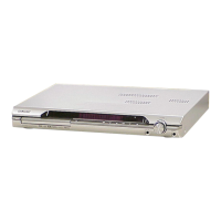
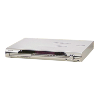
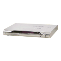
HCD-DZ3K
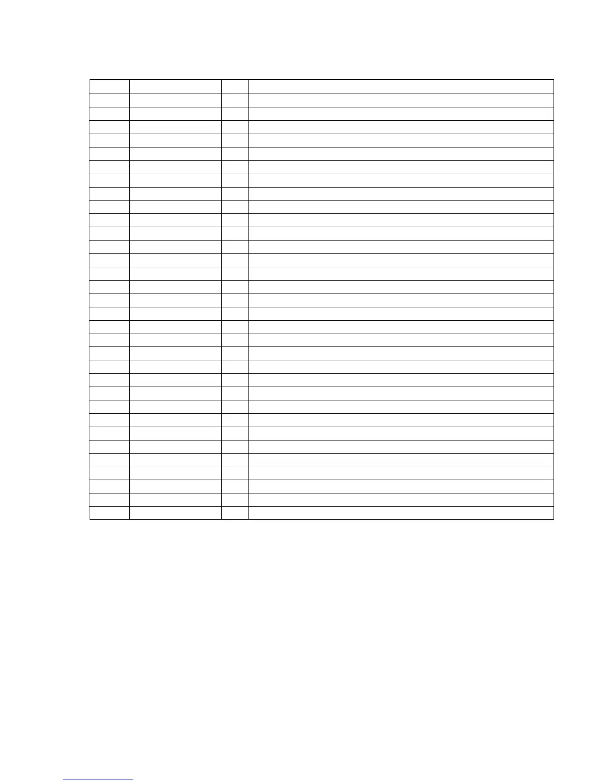
Pin No. Pin Name I/O Description
225 SDPIF — SPDIF output (not used)
226 RFGND18 — Ground terminal
227 RFVDD18 — Power supply (RF+1.8V)
228 XTALO O Oscillator output signal (27MHz)
229 XTALI I Oscillator input signal (27MHz)
230 JITFO O RF jitter meter output
231 JITFN I Negative input of operation amplifier for RF jigger meter
232 PLLVSS — Ground terminal
233 IDAC — Not used
234 PLLVDD3 — Power supply (RF+3.3V)
235 LPFON O Negative output of loop filter amplifier
236 LPFIP I Positive input of loop filter amplifier
237 LPFIN I Negative input of loop filter amplifier
238 LPFOP O Positive output of loop filter amplifier
239 VDD3 I Power supply (RF+3.3V)
240 NC I Not used
241 VSS — Ground terminal
242 NC — Not used
243 NC — Not used
244 RFVDD3 — Power supply (RF+3.3V)
245 RFRPDC I RFRP signal input
246 RFRPAC I RFRP signal input
247 HRFZC I High frequency RF ripple zero crossing
248 CRTPLP O Defect level filter capacitor connecting
249 RFGND — Ground terminal
250 NC — Not used
251 NC — Not used
252 OSP O RF offset cancellation capacitor connecting
253 OSN I RF offset cancellation capacitor connecting
254 RFGC O RF offset loop capacitor connecting for DVD-ROM
255 IREF I Current reference input (not used)
256 AVDD3 — Power supply (RF+3.3V)