1919
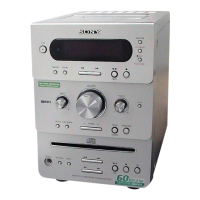
HCD-GP6V
SECTION 7
DIAGRAMS
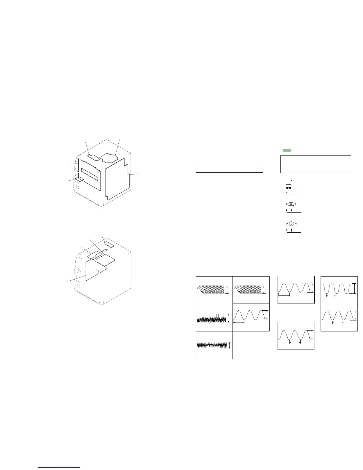
• Circuit Boards Location
For Schematic Diagrams.
Note:
• All capacitors are in µF unless otherwise noted. (p: pF)
50 WV or less are not indicated except for electrolytics and
tantalums.
• All resistors are in Ω and
1
/
4
W or less unless otherwise
specified.
• f : internal component.
• 5 : fusible resistor.
• C : panel designation.
• A : B+ Line.
• H : adjustment for repair.
•Voltages and waveforms are dc with respect to ground un-
der no-signal (detuned) conditions.
no mark: CD PLAY
( ): TAPE REC
•Voltages are taken with a VOM (Input impedance 10 MΩ).
Voltage variations may be noted due to normal production
tolerances.
•Waveforms are taken with a oscilloscope.
Voltage variations may be noted due to normal production
tolerances.
• Circled numbers refer to waveforms.
• Signal path.
F : TUNER (FM/AM)
J : CD PLAY
E : TAPE PLAY
a : REC
j : AUX (VIDEO) IN
L : VIDEO OUT
•Abbreviation
EA : Saudi Arabia model
MY : Malaysia model
SP : Singapore model
For Printed Wiring Boards.
Note:
• X : parts extracted from the component side.
• Y : parts extracted from the conductor side.
• W : indicates side identified with part number.
• f : internal component.
• : Pattern from the side which enables seeing.
(The other layers' patterns are not indicated.)
THIS NOTE IS COMMON FOR PRINTED WIRING BOARDS AND SCHEMATIC DIAGRAMS.
(In addition to this, the necessary note is printed in each block.)
Note: The components identified by mark 0 or dotted
line with mark 0 are critical for safety.
Replace only with part number specified.
Caution:
Pattern face side: Parts on the pattern face side seen from
(Side B) the pattern face are indicated.
Parts face side: Parts on the parts face side seen from
(Side A) the parts face are indicated.
• Indication of transistor.
C
B
These are omitted.
E
Q
B
These are omitted.
CE
Q
B
These are omitted.
CE
Q
MAIN board
BD board
LOADING board
CONTROL board
PHONE board
V-OUT BOARD
MIC/ECHO BOARD
VCD BOARD
POWER BOARD