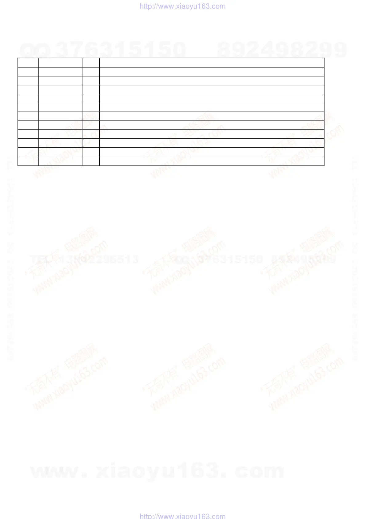
44
HCD-GP7
Pin No.
54
55
56
57
58
59
60
61
62
63
64
I/O
I
I
–
O
I
–
O
–
I
O
–
Pin Name
BOOT/IO6
TXO/IO7
VSSP
PDO
VCOI
VDDP
CKO
VDDX
XI
XO
VSSX
Description
Terminal for test/SUBQ interface frame sync input (fixed at “L”)
Flag signal input 2/SUBQ interface block sync input (fixed at “L”)
Ground for VCO circuit
PLL phase error detection signal output
VCO control voltage input
Power supply (2.5V) for VCO circuit
External clock output
Power supply (2.5V) for oscillation circuit
Resonator terminal (input)
Resonator terminal (output)
Ground for oscillation circuit
w
w
w
.
x
i
a
o
y
u
1
6
3
.
c
o
m
Q
Q
3
7
6
3
1
5
1
5
0
9
9
2
8
9
4
2
9
8
T
E
L
1
3
9
4
2
2
9
6
5
1
3
9
9
2
8
9
4
2
9
8
0
5
1
5
1
3
6
7
3
Q
Q
TEL 13942296513 QQ 376315150 892498299
TEL 13942296513 QQ 376315150 892498299
http://www.xiaoyu163.com
http://www.xiaoyu163.com