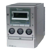
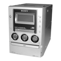
HCD-MG110/MG310AV
4848
7-26. IC PIN FUNCTION DESCRIPTION
•
Pin No. Pin Name I/O Description
1SQSOO
Subcode Q data output to the system controller (IC801)
2SQCKI
Subcode Q data reading clock signal input from the system controller (IC801)
3 XRST I
System reset signal input from the system controller (IC801) “L”: reset
4SYSMI
Analog line muting on/off control signal input terminal “H”: line muting on
Not used (fixed at “L”)
5 DATA I
Command serial data input from the system controller (IC801)
6 XLAT I
Command latch pulse input from the system controller (IC801)
7 CLOK I
Command serial data transfer clock signal input from the system controller (IC801)
8 SENS O
Internal status monitor output to the system controller (IC801)
9 SCLK I
SENSE serial data reading clock input from the system controller (IC801)
10 VDD —
Power supply terminal (+5V) (digital system)
11 ATSK I/O
Input pin for anti-shock Not used (fixed at “L”)
12 SPOA I
Microcomputer escape interface input A terminal Not used (fixed at “L”)
13 SPOB I
Microcomputer escape interface input B terminal Not used (fixed at “L”)
14 XLON O
Microcomputer escape interface output terminal Not used (open)
15 WFCK O
WFCK output terminal Not used (open)
16 XUGF O
Not used (open)
17 XPCK O
Not used (open)
18 GFS O
Not used (open)
19 C2PO O
Not used (open)
20 SCOR O
Subcode sync (S0+S1) detection signal output to the system controller (IC801)
21 COUT I/O
Numbers of track counted signal input/output terminal Not used (open)
22 MIRR I/O
Mirror signal input/output terminal Not used (open)
23 DFCT I/O
Defect signal input/output terminal Not used (open)
24 FOK I/O
Focus OK input/output terminal Not used (open)
25 LOCK I/O
GFS is sampled by 460 Hz “H” when GFS is “H” Not used (open)
26 MDP O
Spindle motor (M101) servo drive signal output to the BA5974FP (IC102)
27 SSTP I
Limit in detect switch (S101) input terminal
28 SFDR O
Sled servo drive PWM signal (+) output to the BA5974FP (IC102)
29 SRDR O
Sled servo drive PWM signal (–) output to the BA5974FP (IC102)
30 TFDR O
Tracking servo drive PWM signal (+) output to the BA5974FP (IC102)
31 TRDR O
Tracking servo drive PWM signal (–) output to the BA5974FP (IC102)
32 FFDR O
Focus servo drive PWM signal (+) output to the BA5974FP (IC102)
33 FRDR O
Focus servo drive PWM signal (–) output to the BA5974FP (IC102)
34 VSS —
Ground terminal (digital system)
35 TEST I
Input terminal for the test (fixed at “L”)
36 TES1 I
Input terminal for the test (fixed at “L”)
37 XTSL I
Input terminal for the system clock frequency setting “L”: 45.1584 MHz, “H”: 22.5792 MHz
(fixed at “L” in this set)
38 VC I
Middle point voltage (+2.5V) input from the CXA2581N (IC103)
39 FE I
Focus error signal input from the CXA2581N (IC103)
40 SE I
Sled error signal input from the CXA2581N (IC103)
41 TE I
Tracking error signal input from the CXA2581N (IC103)
42 CE I
Command chip enable signal input from the CXA2581N (IC103)
CD BOARD IC101 CXD3017Q
(DIGITAL SIGNAL PROCESSOR, DIGITAL SERVO PROCESSOR, DIGITAL FILTER, D/A CONVERTER)
Pin No. Pin Name I/O Description
43 RFDC I
RF signal input from the CXA2581N (IC103)
44 ADIO O
Monitor output of the A/D converter input signal Not used (open)
45 AVSS0 —
Ground terminal (digital system)
46 IGEN I
Stabilized current input for operational amplifiers
47 AVDD0 —
Power supply terminal (+5V) (digital system)
48 ASYO O
Playback EFM full-swing output terminal
49 ASYI I
Playback EFM asymmetry comparator voltage input terminal
50 BIAS I
Playback EFM asymmetry circuit constant current input terminal
51 RFAC I
EFM signal input from the CXA2581N (IC103)
52 AVSS3 —
Ground terminal (digital system)
53 CLTV I
Internal VCO control voltage input of the playback master PLL
54 FILO O
Filter output for master clock of the playback master PLL
55 FILI I
Filter input for master clock of the playback master PLL
56 PCO O
Phase comparison output for master clock of the playback EFM master PLL
57 AVDD3 —
Power supply terminal (+5V) (digital system)
58 VSS —
Ground terminal (digital system)
59 VDD —
Power supply terminal (+5V) (digital system)
60 DOUT O
Digital audio signal output to the DIGITAL OUT (CD) (IC361)
61 LRCK O
L/R sampling clock signal (44.1 kHz) output terminal Not used (open)
62 PCMD O
D/A interface serial data output terminal Not used (open)
63 BCK O
Bit clock signal (2.8224 MHz) output terminal Not used (open)
64 EMPH O
De-emphasis control signal output terminal Not used (open)
65 XVDD —
Power supply terminal (+5V) (crystal oscillator system)
66 XTAI I
System clock input terminal (16.9344 MHz)
67 XTAO O
System clock output terminal (16.9344 MHz)
68 XVSS —
Ground terminal (crystal oscillator system)
69 AVDD1 —
Power supply terminal (+5V) (analog system)
70 AOUT1 O
L-ch analog audio signal output terminal
71 AIN1 I
L-ch operational amplifiers input terminal
72 LOUT1 O
L-ch line output terminal
73 AVSS1 —
Ground terminal (analog system)
74 AVSS2 —
Ground terminal (analog system)
75 LOUT2 O
R-ch line output terminal
76 AIN2 I
R-ch operational amplifiers input terminal
77 AOUT2 O
R-ch analog audio signal output terminal
78 AVDD2 —
Power supply terminal (+5V) (analog system)
79 RMUT O
R-ch line muting on/off control signal output terminal Not used (open)
80 LMUT O
L-ch line muting on/off control signal output terminal Not used (open)
 Loading...