70
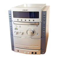
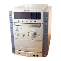
HCD-NXM2D
Pin No. Pin Name I/O Description
58 VDDS — Power supply (+5V)
59, 60 HA0, HA2 I Not used (Pull up)
61 VSS — Ground (open)
62, 63 HCS0, HCS1 I Not used
64 VDD — Power supply (+3.3V)
65 DASP I/O Not used
66 to 69 MDB0 to MDB3 I/O Two-way data bus with the D-RAM
70 VSS — Ground
71 MDB4 I/O Two-way data bus with the D-RAM
72 VDD5V — Power supply (+5V)
73 to 75 MDB5 to MDB7 I/O Two-way data bus with the D-RAM
76 XMWR O Write enable signal output to the D-RAM
77 VDD — Power supply (+3.3V)
78 XRAS O Row address strobe signal output to the D-RAM
79, 80 MA0, MA1 O Address signal output to the D-RAM
81 VSS — Ground
82 to 87 MA2 to MA7 O Address signal output to the D-RAM
88 VDD — Power supply (+3.3V)
89 MA8 O Address signal output to the D-RAM
90 VSS — Ground
91 MA9/MNT0 O Address signal output to the D-RAM
92 MNT1/MNT1 O EEPROM ready signal output to CXP973064-245R
93 MNT2/MNT2 O Address signal output to the D-RAM (not used)
94 XMOE O Output enable signal output to the D-RAM
95 XCAS O Column address strobe signal output to the D-RAM
96, 97 MDB8, MDB9 I/O Two-way data bus with the D-RAM
98 VSS — Ground
99 MDBA I/O Two-way data bus with the D-RAM
100 VDD — Power supply (+3.3V)
101, 102 MDBB, MDBC I/O Two-way data bus with the D-RAM
103 VDD5V — Power supply (+5V)
104 to 106 MDBD to MDBF I/O Two-way data bus with the D-RAM
107 GFS O Guard frame sync signal output to CXP973064-245R
108 VSS — Ground
109 APEO O Absolute phase error signal output
110 VDD — Power supply (+3.3V)
111 DASYO O RF binary signal output
112 GNDA5 — Ground
113, 114 ASF1, AFS2 — Filter connected terminal for selection the constant asymmetry compensation
115 DASYI I Analog signal input after integrated from the RF binary signal
116 RFDCC I Input terminal for adjusting DC cut high-pass filter for RF signal
117 RFIN I RF signal input from the DVD/CD RF amplifier
118, 119 VCCA5, VCCA4 — Power supply (+3.3V)
120 VCOR1 — VCO oscillating range setting resistor connected
121 VCOIN I VCO input
122, 123 GNDA4, GNDA3 — Ground
124 LPF5 O Signal output from the operation amplifier from PLL loop filter
125 VC1 I Middle point voltage (+1.65V) input
126, 127 LPF2, LPF1 I Inverted signal input to the operation amplifier from PLL loop filter
 Loading...