71
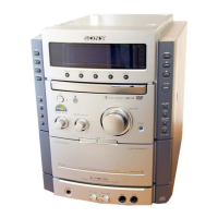
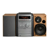
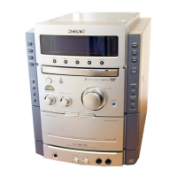
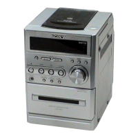
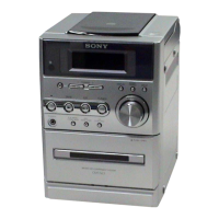
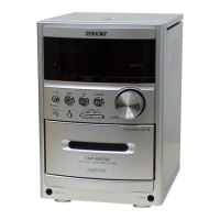
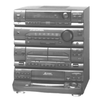
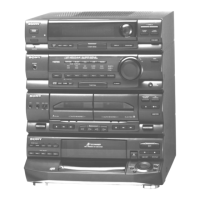
HCD-NXM2D
Pin No. Pin Name I/O Description
128, 129 VCCA3, VCCA2 — Power supply (+3.3V)
130 PDO O Signal output from the charge pump for phase comparator
131 PDHVCC I Middle point voltage input terminal for RF PLL
132 FDO O Signal output from the charge pump for frequency comparator
133, 134 GNDA2, GNDA1 — Ground
135 SPO O Spindle motor control signal output to FAN8035L
136 VC2 I Middle point voltage (+1.65V) input
137 MDIN2 I Spindle motor servo drive signal input
138 MDIN1 I MDP input
139 VCCA1 — Power supply (+3.3V)
140 CLVS O Control signal output for selection the spindle control filter constant at CLVS
141 VSS — Ground
142 MDSOUT O Frequency error output terminal of internal CLV circuit
143 VDD — Power supply (+3.3V)
144 MDPOUT O Phase error output of internal CLV circuit
145 DEFECT I Defect signal input (Not used)
146 GSCOR I Guard subcode sync (S0+S1) detection signal input from CXD3068Q
147 EXCK O Subcode serial data reading clock signal output to CXD3068Q
148 SBIN I Subcode serial data input from CXD3068Q
149 VSS — Ground
150 SCOR I Subcode sync (S0+S1) detection signal input from CXD3068Q
151 WFCK I Write frame clock signal input from CXD3068Q
152 VDD5V — Power supply (+5V)
153 XRCI I Not used (Pull down)
154 VDDS — Power supply (+5V)
155 C2PO I C2 pointer signal input from CXD3068Q
156 VDD — Power supply (+3.3V)
157 DBCK O Bit clock signal (2.8224 MHz) output (Not used)
158 BCLK I Bit clock signal (2.8224 MHz) input from CXD3068Q
159 DDAT O PCM data (Not used)
160 MDAT I Serial data input from CXD3068Q
161 VSS — Ground
162 DLRC O L/R sampling clock signal (Not used)
163 LRCK I L/R sampling clock signal (44.1 kHz) input from CXD3068Q
164 XRST I Reset signal input from CXP973064-245R “L”: reset
165 IFS0 I Not used (connected to ground)
166 IFS1 I Not used (connected to VDD)
167 XTAL I 33.8688 MHz clock signal input from SM8707GV
168 VSS — Ground
169 XTA2 O System clock output (33.8688 MHz)
170 XTA1 I System clock input (33.8688 MHz)
171 VDD — Power supply (+3.3V)
172 to 176 D0 to D4 I/O Two-way data bus with the CXP973064-245R