100
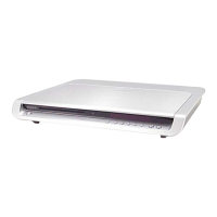
HCD-SR4W
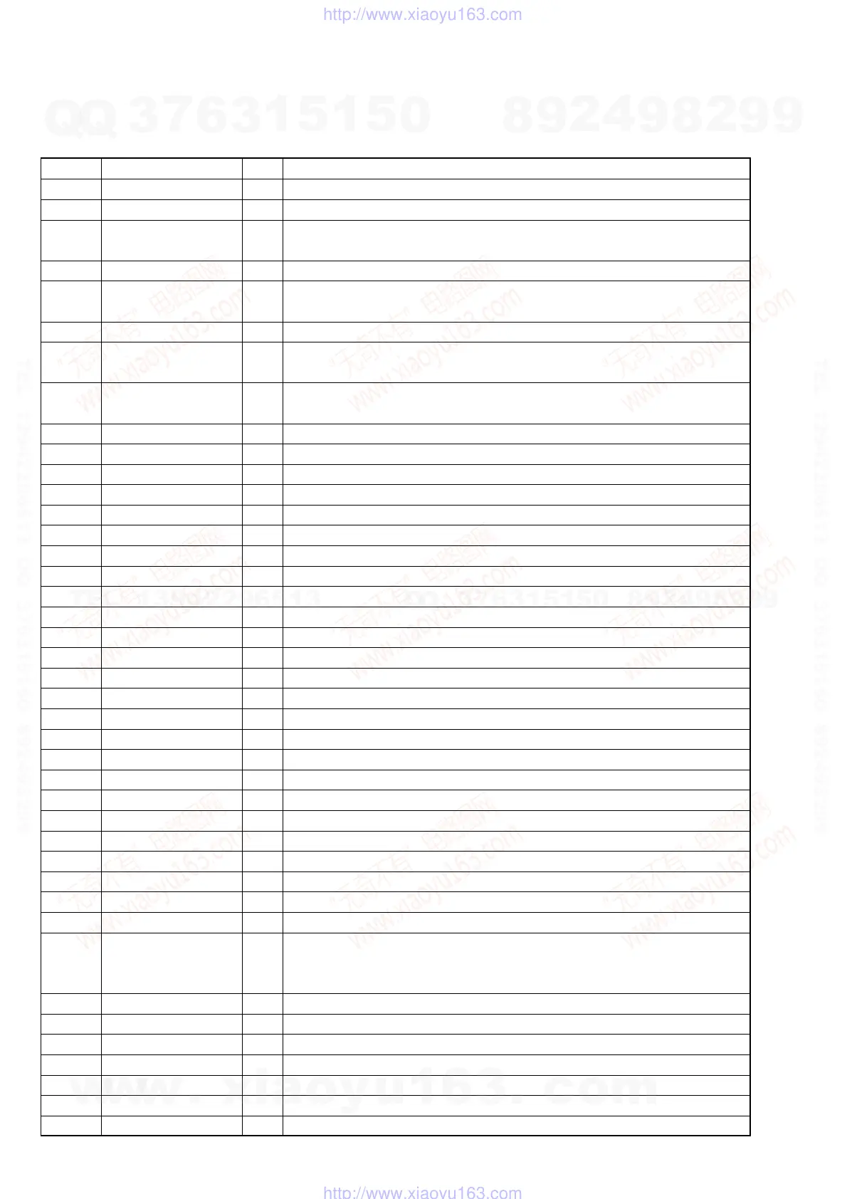
DMB08 BOARD IC901 uPD703033BYGF-M59-3BA-A (SYSTEM CONTROLLER)
Pin No. Pin Name I/O Description
1DAMP-DATA O Serial data output to the stream processors
2DAMP-CLK O Serial data transfer clock signal output to the stream processors
3 I2C-DATA I/O
Communication data bus with the DVD system processor and mechanism
controller
4 CQ-RST O Reset signal output to the DVD system processor “L”: reset
5 I2C-CLK I/O
Communication data reading clock signal input or transfer clock signal output
with the DVD system processor and mechanism controller
6 DSP-DO I Write data input from the audio digital signal processor
7 DIG-DI O
Read data output to the digital audio interface IC, audio digital signal processor
and D/A converter
8DIG-CLK O
Clock signal output to the digital audio interface IC, audio digital signal processor
and D/A converter
9 EVDD — Power supply terminal (+5V)
10 EVSS — Ground terminal
11 P-PWM O PWM voltage control signal output
12 DSP-RST O Reset signal output to the audio digital signal processor “L”: reset
13 DSP-PM O PLL reset signal output to the audio digital signal processor “L”: reset
14 DSP-CS O Chip select signal output to the audio digital signal processor
15 DSP-HACN I Acknowledge signal input from to the audio digital signal processor
16 DSP-BST O Boot strap signal output to the audio digital signal processor
17 DSP-GP9 I Decode signal input from to the audio digital signal processor
18 DIR-ZERO I Audio serial data input from the digital audio interface IC
19 DIR-ERR I PLL lock error and data error flag input from the digital audio interface IC
20 DIR-CE O Chip enable signal output to the digital audio interface IC
21 VPP — Power supply terminal (for programming) Not used
22 DIR-XST I Source clock switching monitor input from the digital audio interface IC
23 DIR-AD O Muting signal output
24 DIR-XMODE O System reset signal output to the digital audio interface IC “L”: reset
25 DIRDO I Write data input from the digital audio interface IC
26 DAMP-RST O Reset signal output to the stream processors “L”: reset
27 GP12 — Not used (fixed at “L”)
28 DAMP-MUTEN O Muting on/off control signal output to the stream processors “H”: muting on
29 CS1 O Chip select signal output to the stream processor (for front L-ch and R-ch)
30 CS2 O Chip select signal output to the stream processor (for center and woofer)
31 CS3 O Chip select signal output to the stream processor (for rear L-ch and R-ch)
32 DAC-CS O Chip select signal output to the D/A converter
33 AD-RST O Reset signal output to the A/D converter and D/A converter “L”: reset
System reset signal input “L”: reset
34 RESET I For several hundreds msec. after the power supply rises, “L” is input, then it
changes to “H”
35 XT1 I Sub system clock input terminal Not used (open)
36 XT2 O Sub system clock output terminal Not used (open)
37 REGC — Capacitance connection terminal
38 X2 O Main system clock output terminal (20 MHz)
39 X1 I Main system clock input terminal (20 MHz)
40 VSS — Ground terminal
41 VDD — Power supply terminal (+5V)
w
w
w
.
x
i
a
o
y
u
1
6
3
.
c
o
m
Q
Q
3
7
6
3
1
5
1
5
0
9
9
2
8
9
4
2
9
8
T
E
L
1
3
9
4
2
2
9
6
5
1
3
9
9
2
8
9
4
2
9
8
0
5
1
5
1
3
6
7
3
Q
Q
TEL 13942296513 QQ 376315150 892498299
TEL 13942296513 QQ 376315150 892498299
http://www.xiaoyu163.com
http://www.xiaoyu163.com