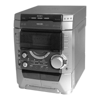
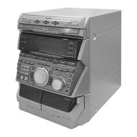
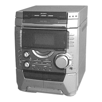
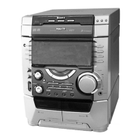
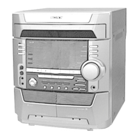
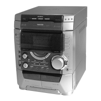
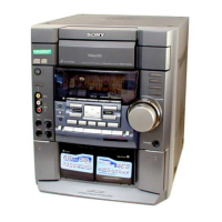
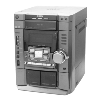
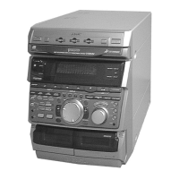
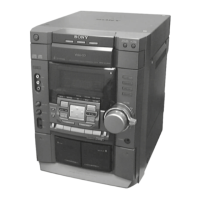
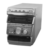
HCD-VX77/VX77J
2323
SECTION 7
DIAGRAMS
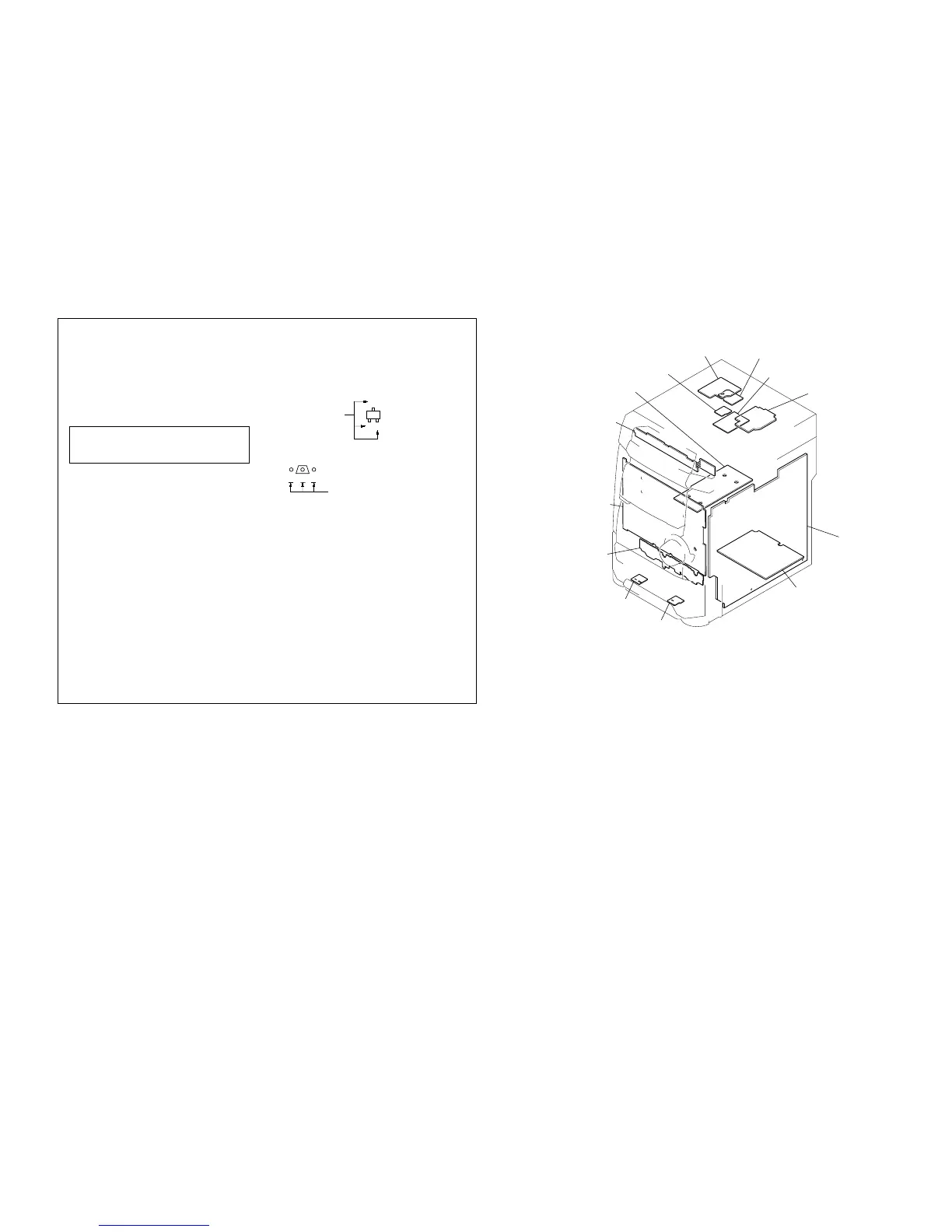
7-1. CIRCUIT BOARD LOCATION
Note on Schematic Diagram:
• All capacitors are in µF unless otherwise noted. pF: µµF
50 WV or less are not indicated except for electrolytics
and tantalums.
• All resistors are in Ω and
1
/
4
W or less unless otherwise
specified.
•
f
: internal component.
• C : panel designation.
Note on Printed Wiring Boards:
• X : parts extracted from the component side.
• b : Pattern from the side which enables seeing.
• Indication of transistor.
Note:
The components identified by mark 0 or dotted line with
mark 0 are critical for safety.
Replace only with part number specified.
• U : B+ Line.
• V : B– Line.
• H : adjustment for repair.
• Voltages and waveforms are dc with respect to ground
under no-signal (detuned) conditions.
• Voltages are taken with a VOM (Input impedance 10 MΩ).
Voltage variations may be noted due to normal produc-
tion tolerances.
• Waveforms are taken with a oscilloscope.
Voltage variations may be noted due to normal produc-
tion tolerances.
• Circled numbers refer to waveforms.
• Signal path.
F : FM
f : AM
E : PB (DECK A)
d : PB (DECK B)
G : REC (DECK B)
J : CD
c : digital out
• Abbreviation
EA : Saudi Arabia model
MY : Malaysia model
SP : Singapore model
TH : Thai model
HK : Hong Kong model
IA : Indonesian model
E3 : Middle and Near East
THIS NOTE IS COMMON FOR PRINTED WIRING BOARDS AND SCHEMATIC DIAGRAMS.
(In addition to this, the necessary note is printed in each block.)
B
These are omitted.
CE
Q
PANEL Board
LEAF SW Board
HEAD (A) Board
HEAD (B) Board
TRANS Board
CD SWITCH Board
VIDEO Board
BD Board
DRIVER Board
MOTOR Board
SENSOR Board
MAIN Board
POWER AMP Board
C
B
These are omitted.
E
Q